


The continuing evolution toward advanced miniature packaging has led to ever increasing printed circuit board (PCB) density and complexity. As the manufacturing process becomes progressively more complicated, there is an ever increasing probability for defects to occur on finished PCB assemblies.
For years the Automated Optical Inspection (AOI) industry has relied solely upon two-dimensional (2D) inspection principles to test the quality of workmanship on electronic assemblies. While advancements in conventional 2D optical inspection have made this technology suitable for detecting such defects as missing components, wrong components, proper component orientation, insufficient solder and solder bridges, there is an inherent limitation in the ability to inspect for co-planarity of ultra-miniature chips, gull-wing leaded devices, BGAs and LED packages.
True co-planarity inspection of these challenging devices is an absolute necessity and literally requires the addition of a third dimension in inspection capability – 3D inspection technology. It is important to understand that there are advantages and disadvantages associated with both 2D and 3D inspection technology. In order to achieve the highest level of quality assurance the AOI system must, therefore, employ a combination of both 2D and 3D inspection technology in a single platform.
Understanding 2D inspection technology
In this day and age, 2D inspection technology is the most widely adapted AOI solution available to electronics manufacturers. The most advanced systems are configured with multiple ultra-high-resolution cameras (10 to 15 megapixels), precision telecentric lenses and multi-tiered lighting technology to properly illuminate regions of interest across the assembly.
The most technologically advanced hardware, however, is not enough. The AOI system must also provide a sophisticated arsenal of 2D inspection algorithms to characterise and inspect for manufacturing defects on finished PCB assemblies. In order to fully understand this technology we must examine both the advantages and disadvantages associated with 2D inspection. These are outlined in Table 1.
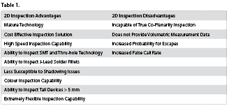
As we can see, although there are some inherent limitations with 2D inspection technology, there are some significant advantages which make 2D inspection an extremely viable technology. Even the simple ability to test for two dimensional component nomenclature and polarity indications is sufficient to make 2D technology an absolute requirement for automated inspection.
Understanding 3D inspection technology
Although 3D inspection technology has existed for many years in the electronic inspection industry, this technology has primarily been reserved for inspecting solder paste depositions on printed circuit boards directly after the screen printing process. Over the past few years, however, 3D inspection has emerged as a viable technology for testing gull-wing and BGA devices as well as a host of other co-planarity sensitive circuitry on finished PCB assemblies. Of course, the main reason for the industry trend toward 3D inspection technology is to compensate for the limitations of conventional 2D inspection.
There are basically two different methodologies by which 3D inspection is employed in AOI machines. The first is laser measurement and the second is multi-frequency moiré phase shift image processing.
Laser measurement methodology uses a laser subsystem to scan across gull-wing lead tips as well as provide 3D measurement of BGA and other height sensitive devices. This proven methodology works very well for detecting co-planarity defects that may otherwise be missed with conventional 2D inspection. Unfortunately, this technology does not provide volumetric measurement of a given region of interest and is primarily reserved for testing gull-wing leaded devices and BGAs. Another limitation of laser measurement is the inability to inspect solder fillets post reflow.
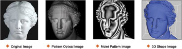
Multi-frequency moiré is by far the most advanced methodology for testing true co-planarity of virtually any given region of interest on the PCB. Moiré 3D phase shift image processing is a methodology by which a single or multiple projectors are used to project a shifting pattern of lines on a given region of interest. A digital camera then captures the image of deformed lines as they are shifted across the test surface. By applying phase shift analysis and phase unwrapping techniques, the 3D profile of the test surface can be reconstructed for precise measurement (see Figure 1).
Multi-frequency moiré takes this one step further in that two or more line patterns of differing frequencies are projected onto a given test surface in order to characterise objects of varying heights, as shown in Figure 2.
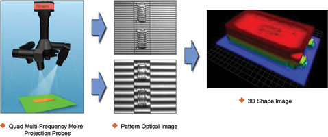
The most advanced systems employ a series of four or more digital multi-frequency moiré projection probes to yield precise height measurement data which may then be used to detect lifted component and lifted lead defects as well as provide solder volumetric data post reflow. The fact that the probes are digitally programmable means that the pattern frequency may be altered via software to provide the ultimate in inspection flexibility. The alternative methodology uses two fixed frequency patterns which may prove limited for some applications.
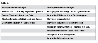
Once again, in order to fully understand 3D inspection we must examine the advantages and disadvantages associated with this technology. These are outlined in Table 2.
After carefully reviewing the advantages and disadvantages of both 2D inspection and 3D inspection it becomes increasingly evident that neither technology is completely capable of addressing the full complement of inspection requirements associated with the complexity of current and future electronic assemblies. In order to successfully cover the full range of inspect requirements without compromise, the AOI machine must provide both 2D and 3D inspection capability in a single platform.
The most technologically advanced AOI systems must essentially provide the following:
• A state of the art 2D hardware/software engine configured with a minimum of five ultra-high resolution cameras, precision telecentric lens architecture and a multi-tiered lighting system combined with a sophisticated feature set of algorithms designed to leverage the various advantages associated with a 2D inspection technology.
• A 3D subsystem with either laser measurement or multi-frequency moiré capability. In the case of the latter, more desirable 3D inspection solution, the system must be configured with four or more multi-frequency moiré projection probes to provide highly accurate 3D imaging from which the system may extract precise volume and shape characteristics for any given region of interest on the finished PCB assembly.
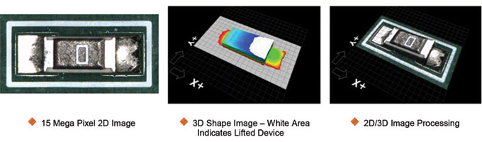
The end result is a highly accurate quality assurance system which combines the advantages of 2D inspection technology with the advantages of 3D inspection technology without compromise. Figure 3 shows the inspection results from one such AOI system configured with a 15 megapixel downward camera with telecentric lens architecture, four 10 megapixel side view cameras, a six tier colour lighting system and a digital multi-frequency quad moiré 3D subsystem.
In summation, the continuing trend toward higher PCB density and the ensuing miniaturisation of electronic packaging technologies has resulted in an unprecedented level of complexity for the manufacturing process. In order to contend with the complexity of today’s PCB assemblies, the AOI system must provide both 2D and 3D inspection capability.
By combining the flexibility and accuracy of 2D inspection technology with the advanced measurement capability of 3D technology, the AOI system becomes an extremely effective tool that will provide manufacturers with a clear view into the manufacturing process, thereby helping them achieve higher operating efficiencies and improved quality.
For more information contact Techmet, +27 (0)11 824 1427, info@techmet.co.za, www.techmet.co.za
| Tel: | +27 11 824 1427 |
| Fax: | +27 11 824 3150 |
| Email: | sales@techmet.co.za |
| www: | www.techmet.co.za |
| Articles: | More information and articles about Techmet |


© Technews Publishing (Pty) Ltd | All Rights Reserved
 printer friendly version