


The challenge of designing robust electronic circuitry often results in a design with a multitude of discrete protection components with associated cost, design time and space additions.
The challenge of designing robust electronic circuitry often results in a design with a multitude of discrete protection components with associated cost, design time and space additions. This article discusses fault protected switch architecture, along with the performance benefits and other advantages it offers versus traditional discrete protection solutions. A novel switch architecture and proprietary high-voltage process that provides industry-leading fault protection, along with the performance required for precision signal chains, is discussed. Analog Devices’ new portfolio of fault protected switches and multiplexers (ADG52xxF and ADG54xxF) uses this technology.
Analog input protection for high-performance signal chains is often a pain point for system designers. There is typically a significant trade-off between analog performance (such as leakage and on-resistance) and the level of protection that can be offered by discrete components.
Replacing the discrete protection components with over-voltage protected switches and multiplexers can offer significant benefits in terms of analog performance, robustness and solution size. The over-voltage protected component sits between sensitive downstream circuitry and the input that is exposed to external stresses. An example of this would be the sensor input terminal in a process control signal chain.
This article details the issues caused by over-voltage events, discusses traditional discrete protection solutions and the associated drawbacks, presents the solution offered by over-voltage protected analog switches including features and system benefits, and finally introduces the industry-leading portfolio of Analog Devices fault protected analog switches.
Over-voltage issues – back to basics
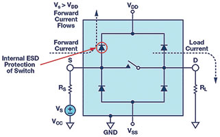
When the input signal applied to a switch exceeds the power supplies (VDD or VSS) by more than a diode drop, the ESD protection diodes within the IC become forward biased and current flows from the input signal to the supplies, as shown in Figure 1. This current could damage the part and may trigger a latch-up event if the current is not limited.
If the switch is unpowered, there are a couple of scenarios that could occur:
1. If the power supplies are floating, the input signal could end up powering the VDD rail through the ESD diodes. In that case, the VDD pin goes to within a diode drop of the input signal. This means the switch would effectively be powered, as would any other components using the same VDD rail. This could lead to unknown and uncontrolled operation of devices in the signal chain.
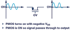
2. If the power supplies are grounded, the PMOS device will turn on with negative VGS so the switch will pass a clipped signal to the output, possibly damaging downstream components that would also be unpowered (see Figure 2). Note: if there are diodes to the supply, they will forward bias and clip the signal to +0,7 V.
Discrete protection solution
Designers traditionally solve input protection issues with discrete protection components. Large series resistors are used to limit the current during a fault, and Schottky or Zener diodes to the supply rails clamp any over-voltage signals. An example of such a protection scheme in a multiplexed signal chain is shown in Figure 3.
However, there are many disadvantages to using these discrete protection components.
1. The series resistor will increase the settling time of the multiplexer and slow down the overall settling time.
2. The protection diodes will introduce additional leakage current and varying capacitance that will impact the precision and linearity of the measurement.
3. There will be no protection in the floating supply condition as the ESD diodes to the supplies won’t provide any clamping protection.
Traditional switch architecture
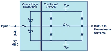
The diagram in Figure 4 gives an overview of a traditional switch architecture. The switch component (on the right hand side of Figure 4) has ESD diodes to each of the supply rails, at both the input and output side of the switch element. The external discrete protection components are shown here as well – the series resistor for current limiting and the Schottky diodes to the supplies for over-voltage clamping. There is often a requirement for a bidirectional TVS for additional protection in harsher environments.
Fault protected switch architecture
The fault protected switch architecture is shown in Figure 5. The ESD diodes at the input side are replaced with a bidirectional ESD cell, so the input voltage range is no longer limited by the ESD diodes to the supply rails. Therefore, the input can see voltages up to the limitation of the process (which is ±55 V for the new fault protected switches from Analog Devices).
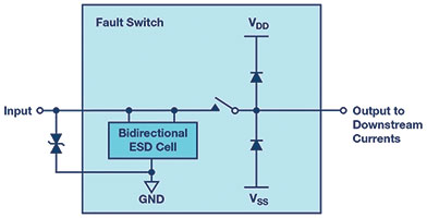
The ESD diodes remain at the output side in most cases as there usually isn’t a requirement for over-voltage protection from the output side. The ESD cell at the input side can still provide excellent ESD protection. The ADG5412F over-voltage fault protected quad SPST switch that uses this type of ESD cell achieves a 5,5 kV HBM ESD rating.
There may still be a requirement for an external TVS or a smaller current limiting resistor for more stringent cases such as IEC ESD (IEC 61000-4-2), EFT or surge protection.
In the case of an over-voltage condition at one of the switch inputs, the affected channel turns off and the input goes high impedance. The leakage will remain low on the other channels, so the remaining channels can continue to operate as normal with minimal impact on performance. This allows for very little compromise between system speed/performance and over-voltage protection.
The fault protected switch can therefore greatly simplify the signal chain solution. The switch over-voltage protection removes the requirement for the current limiting resistors and Schottky diodes in many cases. The overall system performance is no longer limited by external discrete components that typically introduce leakage and distortion into a signal chain.
Analog Devices fault protected switch features
The new portfolio of fault protected switches from Analog Devices are built on a proprietary high-voltage process that provides over-voltage protection up to ±55 V in both the powered and unpowered states. These parts provide industry-leading performance for fault protected switches for precision signal chains.
Latch-up immunity
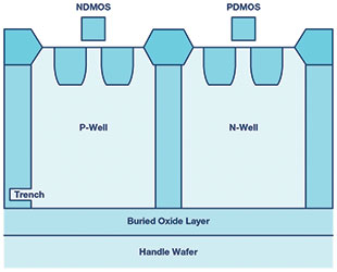
The proprietary high-voltage process is also trench isolated. An insulating oxide layer is placed between NDMOS and the PDMOS transistors of each switch. Parasitic junctions, which occur between the transistors in junction-isolated switches, are eliminated and the result is a switch that is latch-up immune under all circumstances. The ADG5412F, for example, passes a JESD78D latch-up test of ±500 mA for a 1 second pulse width, which is the most stringent test in the specification.
Analog performance
As well as achieving industry leading robustness (over-voltage protection, high ESD rating, known state at power-up without digital inputs present), the new fault protected switches also have industry-leading analog performance. Switch performance as always is a trade-off between low on-resistance and low capacitance/charge injection. The choice of switch usually depends on whether the load is high impedance or low impedance.
Low impedance systems
Low on-resistance parts are usually used in low impedance systems, where the on-resistance of the switch needs to be kept to a minimum. In low impedance systems, such as a power supply or gain stage, the on-resistance and source impedance in parallel with the load can cause gain errors. Even though gain errors can be calibrated out in many cases, the variation of on-resistance (RON) across signal range or between channels produces distortion that cannot be calibrated out. Therefore, low resistance circuits are more subject to distortion errors due to RON flatness and RON variation across channels.
The plot in Figure 7 shows the switch on-resistance of one of the new fault protected switches across the signal range. As well as achieving very low on-resistance, the RON flatness and matching between channels is also excellent. The parts have a patented switch driver design that guarantees a constant VGS voltage and delivers flat RON performance across the input voltage range. The trade-off is a slightly reduced signal range where optimal performance can be achieved, which can be seen from the shape of the RON plots. There can be significant system benefits because of this RON performance in applications sensitive to RON variation or THD.
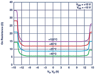
The ADG5404F is the new latch-up immune, over-voltage fault protected multiplexer. Latch-up immune parts and over-voltage protected parts typically have higher on-resistance and worse on-resistance flatness than standard parts.
However, due to the constant VGS scheme used in the ADG5404F design, the RON flatness is actually better even than the ADG1404 (industry-leading low on-resistance) and ADG5404 (latch-up immune, but not over-voltage protected). In many applications, such as RTD temperature measurements, the RON flatness is actually more important than the absolute value of on-resistance so the fault protected switch provides potential for increased performance in these systems.
The typical fault mode for a low impedance system is for the drain output to go open circuit in the case of a fault.
High-impedance systems
Low leakage, low capacitance, low charge injection switches are most commonly used in high-impedance systems. Data acquisition systems are typically high impedance due to amplifier loads on the multiplexer output. Leakage is the dominant source of error in high-impedance circuits. Any leakage currents can lead to significant measurement errors. Low capacitance and low charge injection are also critical for faster settling. This allows for maximum data throughput in a data acquisition system.
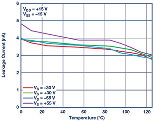
The leakage performance of the new Analog Devices fault protected switches is excellent. In normal operation the leakage current is in the low nA range, which is critical for accurate measurements in many applications. Critically, the leakage performance is also very good even when one of the input channels is in fault. This means that measurements can continue on other channels until the fault is fixed, thereby reducing system downtime. The over-voltage leakage current for the ADG5248F 8:1 multiplexer is shown in Figure 8.
The typical fault mode for a high impedance system is for the drain output to pull to the supply rail in the case of a fault.
Fault diagnostics
Most of the new Analog Devices fault protected switches also feature digital fault pins. The FF pin is a general fault flag, which indicates that one of the input channels is in fault. The specific fault pin (or SF pin) is a pin that can be used to debug which specific input is in fault.
These pins can be useful for fault diagnostics in a system. The FF pin first alerts a user to a fault. The user can then cycle through the digital inputs and the SF pin will identify which particular switch or switches are in fault.
Application examples
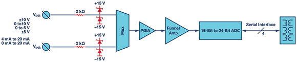
This first application example shown in Figure 9 is a process control signal chain, where a microcontroller is monitoring a number of sensors such as RTD or thermocouple temperature sensors, pressure sensors and humidity sensors. In a process control application, the sensor may be connected at the end of a very long cable in a factory, with the potential for faults along the length of the cable.
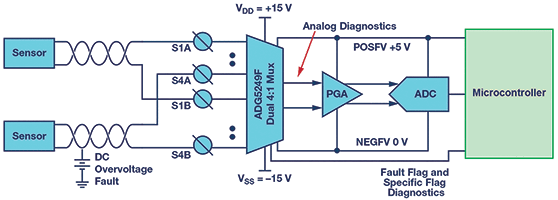
The multiplexer in this case is the ADG5249F, which is optimised for low capacitance and low leakage. Low leakage is important for these types of small signal sensor measurements. The switch operates off ±15 V supplies, while the secondary fault supplies are configured for 5 V and GND to protect the downstream PGA and ADC.
The main sensor signal passes through the multiplexer to the PGA and ADC while the fault diagnostics are sent directly to the microcontroller to provide an interrupt in the case of a fault. The user can therefore be alerted to a fault condition and can determine which of the sensors is in fault. A technician can then be sent out to debug the fault and if necessary replace the sensor or cable in fault.
Because of the industry-leading low fault leakage specification, the other sensors can continue to be monitored even while one of the sensors is down and awaiting replacement. Without such low fault leakage, a fault on one channel could make all of the other channels unusable until the fault is repaired.
The second application example in Figure 10 is a portion of a data acquisition signal chain where the ADG5462F channel protector would add value. In this case there is a PGA with ±15 V supply rails, while the ADC downstream has as input signal range of 0 V to 5 V.
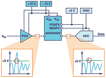
The channel protector sits between the PGA and ADC. It uses the ±15 V supply rails as its primary supplies to achieve optimum on-resistance, and uses 0 V and 5 V for its secondary supply rails. The ADG5462F will allow the signal to pass through in normal operation, but will clamp any over-voltage outputs from the PGA to between 0 V and 5 V to protect the ADC. Therefore, like the previous applications example, the signal of interest is biased in the flat RON region of operation.
Summary
Replacing traditional discrete protection components with over-voltage protected switches and multiplexers can provide many system benefits in a precision signal chain. As well as saving board space, the performance benefits of replacing discrete components can be significant.
Analog Devices has a wide range of over-voltage protected switches and multiplexers. They are built on a proprietary high-voltage and latch-up immune process and provide industry leading performance and features for precision signal chains.
For more information contact EBV Electrolink, +27 (0)21 402 1940, [email protected], www.ebv.com
| Tel: | +27 11 236 1900 |
| Fax: | +27 11 236 1913 |
| Email: | [email protected] |
| www: | www.ebv.com |
| Articles: | More information and articles about EBV Electrolink |


© Technews Publishing (Pty) Ltd | All Rights Reserved
 printer friendly version