


If you are repairing land grid array (LGA) or area array devices, should you print the circuit board or the device terminations?
Either method can work, with your own skills determining which is easier and more repeatable.
Recent hands-on rework workshops proved very successful for the author and delegates reworking these fairly new packages. Special thanks go to TECAN in the UK for making the handheld manual rework foils specifically designed for QFN (quad flat no-lead) and LGA packages. Let us now step through the process in this step-by step-guide.
Firstly, make sure that the solder paste being used in rework is the same as in production. Often a dispense grade with larger ball size or lower metal content is used in repair areas but may not be suitable for stencil printing these fine pitch parts.
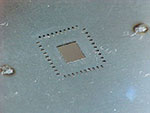
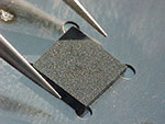
Select a micro stencil for the component footprint for a land grid array; this would normally be 0,004” (100 μm) foil (Figure 1). The stencil apertures for the outer pads are produced as one to one apertures. The centre aperture can be single or multiple apertures to cover between 50% and 60% of the surface area. It is recommended to have the paste printed to the centre of the device, not to the edge of the centre pad.
The stencil, being very thin, has a backing foil of between 0,010” and 0,012” thick and allows the stencil to be used for manual hand printing.
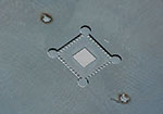
The thicker support foil (Figure 2), prevents the image foil being flexed during printing, which can lead to inconsistent deposits. The support foil also allows the component to be positioned accurately to the terminations (Figure 3).
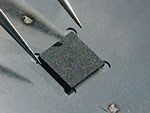
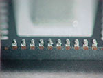
Place the LGA/QFN component into the stencil guide and check the right stencil is being used and the apertures are perfectly aligned with the terminations. One finger can be used to hold the component in position while the stencil is turned over for printing (Figure 4). Alternatively a small piece of Kapton tape can be used to hold the part in position.
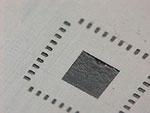
The component can now be printed with solder paste using a small metal rework squeegee blade. It is important to use the blade in the same way as a printer; make sure the paste is rolling and the surface of the stencil is clean after the print stroke. Inspect to confirm that the paste is completely filling the apertures.
Before printing solder paste onto components, try printing paste images onto a flat surface like copper clad laminate, glass or thick white card. This will allow an opportunity to perfect the repair printing process. When the correct technique has been mastered, check the cleanliness of the stencil apertures and base to prevent contaminating the component surface with paste.
Turn the stencil over so the part can be lifted prior to placement (Figure 5). If the component is lifted manually it can be inspected visually prior to placement on the board. If the stencil is going to be located on a rework system the component can be placed automatically, and inspection of the paste deposits can be conducted on the rework system when the component is aligned with the pads prior to placement.
Make sure you check the stencil after use and clean or check for paste remaining in apertures if you intend to print a second device. Paste release from the stencil is just as important as printing in normal manufacture to achieve the best yields.
Another option is to jet print the solder paste directly to the board or on the surface of the component, just like manual printing. There are two or three jetting systems on the market today, one of which is a benchtop system which is perfect to use for rework or bumping packages.
Bumping QFN/LGA packages can improve reliability and decrease voiding during reflow.
For more information visit www.bobwillis.co.uk


© Technews Publishing (Pty) Ltd | All Rights Reserved
 printer friendly version