


The day began not unlike others. Leave home, get a bagel and a large cup of caffeine, and drive to the office. I am the president and CTO of an equipment manufacturing company located in Southern California. Most days begin with a walk through the factory floor, and a short conversation with my management team. This day, however, began with an unusual phone call. The man on the other end of the phone call stated, “I am a lawyer and I need your help”. This was to be an interesting day.
There are several unique words and phrases associated with my business, words not commonly used at cocktail parties or chance encounters with strangers. During my phone call with the lawyer, words and phrases such as ‘dendritic growth’, ‘CAF’ and ‘ECM’ were thrown about. While these words and phrases would certainly be the most uninteresting cocktail party conversation starters, they were music to my ears. You see, my company manufactures equipment that removes process residues from circuit assemblies, as well as machines that test assemblies to quantify the level of cleanliness. Dendritic growth, CAF and ECM are all reasons we are in business.
Here’s the scoop: there were two companies engaged in a lawsuit. The plaintiff was a startup company fuelled by venture capitalist money. They had a product idea associated with transportation technology. This is the point in my story where I should inform the reader that my descriptions of the primary players shall remain intentionally vague as I am bound by a non-disclosure agreement.
The plaintiff created a new technology that consisted of a sensor and a receiver. The sensor would be installed in the ground and send signals to a receiver mounted on a nearby pole above ground. Because the ground-based sensor would not be connected to a power source, it would require a long-life (10 year plus) battery. While the plaintiff had the skillset required to design a functioning circuit and related product, they lacked the ability to produce it. Enter the contract manufacturer (CM), soon to be the defendant.
This part of the story is most likely typical. The intellectual property (IP) owner provided a Statement of Work (SOW) to the CM. The SOW provided the minimum amount of technical detail. The IP owner cited a couple of IPC standards, specified a bill-of-materials including a bare board material described as “down and dirty cheap FR4” (a description that would not serve them well during litigation). The CM ordered bare boards from a Chinese board supplier. Components were ordered and the CM began to produce product for their customer.
The SOW required the following procedures in the production of the assemblies:
• The product required a multi-layer board with the selection ‘standard FR4’ (no slash sheets).
• The assembly would be reflowed using an organic acid (ORH1) lead-free solder paste.
• The assembly would be cleaned using a water-only inline cleaning system.
• After cleaning, a high-mass electrical component would be manually soldered to the assembly using a lead-free solder and no-clean flux. Due to the component’s mass, flux was added to the component via a squeeze-bottle. No further cleaning would be performed.
• Once the assembly was fully assembled (reflowed and hand soldered), a battery would be installed and the assembly would be subjected to thermo-testing. Assemblies were loaded into ovens and function tested at a specified temperature for a specified amount of time. All products were subjected to testing.
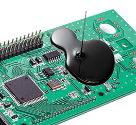
• Successfully tested assemblies would be encapsulated into a hockey-puck sized plastic container using a silicone material.
While these specifications appear to be unexceptional, the list above is missing the vital specifications that sealed the product’s fate. Because this assembly’s sole source of power was a battery, the assembly’s surface cleanliness should have been considered.
Every assembly has a ‘residue tolerance’, a volume of conductive residue that can remain on an assembly while not contributing to electro-chemical migration (ECM). The further components are from each other, the more ionic residue can be tolerated.
Additionally, the less an assembly is exposed to in-use moisture, the more residue it can tolerate. Because the assembly is exclusively powered by a battery, and because the assembly would be potted (battery and all) and buried in the ground, and therefore would not afford easy access to change the battery, and because the assembly was highly miniaturised, its tolerance for residues was low. Despite these facts, two cleaning miscalculations were made.
The first miscalculation was to clean using just water. Removing harmful ionic residues from assemblies requires a knowledge of the various residue species common to electrical assemblies. One must consider process residues from the original board fabrication process. These include etch residues, developer chemicals, water quality rinses for inner layers, water quality rinses for outer layers, HASL fluids (HO) and final rinses, and alkaline cleaners.
Component fabrication residues must also be considered, including plating bath residues, water quality rinses, de-flashing chemicals, mould release agents, pre-plating oxide cleaning and pre-tinning flux residues. Additionally, assembly associated residues such as solder paste, flux – wave, cored solder, reworked/repaired fluxes, cleaning chemicals, water rinse quality and rework cleaner must be considered. Finally, human-based residues such as finger oils, food particles, hand creams/moistures, etc. can be transferred to an assembly.
The various residue species listed above fall into one of two categories: polar and non-polar. Polar residues are hydrophilic and therefore soluble in water. Non-polar residues are hydrophobic and therefore not soluble in water. The list of possible assembly residues contains both polar and non-polar contamination species. Cleaning with water only will, at best, only remove polar contaminants and leave behind all non-polar contaminants, which is exactly what happened in this scenario.
To make matters worse, after the assemblies were cleaned using just water, a physically large component was hand-soldered to the assembly using no-clean (REM1) flux. Even though extra flux was added via a squeeze bottle to the assembly, no additional cleaning was provided. There were two issues with the installation of this large component.
First, because of the component’s mass, extra flux was required for proper wetting. So much flux was applied that excess flux travelled to parts of the component and assembly that were not exposed to the heat of the soldering iron. This allowed for the flux’s activators to remain intact rather than being burned off during the soldering process. Because the IP owner (author of the SOW) believed all residues from no-clean flux were inert and harmless, the excess flux residues (and the activators contained therein) were allowed to remain.
Another omission in the process standard was any form of bake-out. While subjecting boards or assemblies to a bake-out is frequently not required, in this case there were multiple reasons to conduct a bake-out. First, circuit boards used in the project featured a multi-layer design. Multi-layer boards can pick up moisture from various steps along the way, including fabrication, transportation, storage and wash processes. In this case, the boards were fabricated in China and sent by ocean freight to the United States. Once the boards were received by the contract manufacturer, no special (dry box) storage was provided. There was also no evidence of a first-in first-out (FIFO) inventory strategy.
Additionally, the assemblies were subjected to a water-based cleaning process utilising an inline cleaning system equipped with a common airknife drying system. Airknife drying systems are effective at removing most of the surface moisture added to the assembly during a wash process. They are not normally effective at removing entrapped moisture or moisture within the board layers.
The absence of a baking process was justified by the IP owner because the assembly would eventually be encapsulated in silicone, allegedly protecting it from environmental moisture in the field. While this belief is partially true, the application of this logic sealed the fate of the assembly by likewise sealing in all the sins of the assembly process. More on that later.
After the assembly was complete and subjected to a thermo-cycling quality control procedure, it was sent to a contract conformal coating company. Citing best practices, the contract conformal coating company recommended to the IP owner that the assemblies be cleaned and baked prior to coating. This suggestion was refused by the IP owner. At one point, the thermo-cycling equipment failed and was unable to properly perform the required quality tests. The IP owner waived the test requirements and rejected the pre-encapsulation cleaning and baking suggestions in the interest of maintaining production quotas, in part because their investors were pressuring them to ship product. The repercussions of these decisions, in totality, were about to become evident.
Several design and production decisions contributed to a disastrous outcome. Just months after the product was shipped to customers and installed several inches below city streets, the batteries began to fail. The same batteries that were expected to last 10 years were rapidly draining, and were dead within a few months. By the time everyone agreed there was a problem, sixty thousand units needed to be recalled. The IP owner believed the contract manufacturer was at fault and initiated a lawsuit against the CM. This led to the hiring of various experts to determine the cause of the product failures. Here were our findings:
Issue #1: CAF
The multi-layer circuit boards contained micro-cracks beneath the surface of the board, emanating from the drilled through-holes and vias. Plating solution used to copper-plate the through-holes and vias entered the micro-cracks. This is not an unusual phenomenon. It can be caused by dry-weave, drilling of through-holes, and multiple thermo-excursions.
Electrical current, conductive solution (plating fluids) and moisture combined to exploit the micro-cracks and form conductive anodic filaments (CAF). CAF is a form of electro-chemical migration (ECM) that occurs beneath the board’s surface. The formation of CAF allowed unwanted current flow between anodes and cathodes, reducing the dielectric properties of the board, resulting in premature battery drain and, in some cases, direct shorts.
Remedies
There were several missed opportunities to eliminate the possibility of CAF failures. First, because these assemblies were to be installed in harsh environments, and because they would not be easily accessed once installed, and because the product was exclusively powered by a battery, more caution should have been exercised in the selection of board materials. There are CAF-resistant laminates available which would have reduced the likelihood of CAF.
Second, the absence of a bake-out process contributed to CAF. As previously stated, CAF requires four elements: electrical current, a pathway (micro-cracks), conductive materials (plating solutions) and moisture. Proper baking would have removed the moisture and eliminated the possibility for CAF to form.
Next, circuit design can either increase or decrease the propensity for CAF. Voltage, component density, via locations and other factors all influence CAF. IPC TM650 2.6.25 outlines CAF testing, and failure analysis laboratories offer specialised CAF prediction testing. Depositions of the design engineers confirmed that there was no knowledge of CAF, nor any design or process considerations regarding CAF
Issue #2: dendritic growth
The presence of dendritic growth was evidenced in many of the failed assemblies. Dendritic growth is another form of ECM. Unlike CAF, dendrites grow on the board’s surface, between cathodes and anodes. Dendritic growth requires three elements: electrical current, conductive materials and moisture. The conductive materials required for dendritic growth include flux residues as well as residues from board fabrication, component fabrication and the assembly process.
Remedies
The removal of residues from the assembly would have eliminated the possibility of dendritic growth or other surface related ECM issues. The contract manufacturer, at the direction of the IP owner, cleaned the assemblies after reflow using a water-only cleaning process. This allowed all non-polar residues to remain on the assembly. The implementation of a cleaning process with a chemical additive would have allowed all residue species, polar and non-polar, to be removed.
Additionally, the installation of an additional component after cleaning allowed flux residue to remain on the assembly. The application of excess volumes of flux allowed much of the flux’s activators to remain on the assembly. In this case, there are two remedies. The residues could have been subjected to a manual cleaning process (the component was not compatible with water). Alternatively, the assembler could have minimised the volume of flux added to the assembly, ensuring all of the no-clean flux that was added was adequately heat activated, burning off harmful flux activators.
Issue #3: no bake-out
The IP owner believed because the assembly would be encapsulated in silicone, it would be protected from moisture and other harsh substances. Unfortunately, encapsulation had the opposite effect. Encapsulation actually sealed in moisture. Because the board was never subjected to a formal bake-out procedure prior to encapsulation, moisture was sealed in. There was enough moisture to exploit the board’s micro-cracks, plating solution and electrical current to result in CAF failures. There was also enough moisture to combine with electrical current and flux and other process residues to allow surface-level dendritic growth to occur.
Remedies
In this case, even with excessive residues allowed to remain on the assembly, and even with the board’s micro-cracks, an effective bake-out procedure just prior to encapsulation would have decreased and possibly even eliminated all ECM related failure possibilities.
The bottom line
I am sure we have all been in a situation where we were asked to provide a service or a product in a manner that was not correct. We may be asked to take shortcuts or produce a product or service in a manner that represents less than best practices. While few of us would knowingly agree to build products we know will fail, it is easier to, over time, agree to small changes. Perhaps we are requested to shorten testing time or skip a bake-out process or purchase cheaper materials, little by little jeopardising the product’s long term reliability.
It is amazing how these two companies didn’t have the time to do it right, but had the time to do it over. Sometimes the most profitable word in business is “no”.
| Tel: | +27 11 869 0049 |
| Fax: | +27 83 232 7904 |
| Email: | mykay@iafrica.com |
| www: | www.mykaytronics.co.za |
| Articles: | More information and articles about MyKay Tronics |


© Technews Publishing (Pty) Ltd | All Rights Reserved
 printer friendly version