


In the 16 February 2011 issue of Dataweek, the article entitled ‘Microsectioning improves PCB quality’ covered the necessity of using microsections as a method of quality control.
As promised in that article, we will now go into some detail about the types of faults that the microsection experts look for. But first, a quick recap on microsections.
What exactly is a microsection?
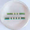
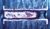
Microsections are tiny samples taken from multilayer PCBs when each order comes off the line. A panel is taken from the overrun on each batch and microsections are taken from two PCBs at opposing corners of the panel (Figures 1a and 1b).
Multilayer PCBs are made up of extremely thin layers of fibreglass and copper. Dimensions and tolerances are measured in microns and, as designs and technology advance, PCBs are expected to accommodate more technology on smaller surface areas. With layers so thin that they are barely visible to the naked eye, it takes microscopic examination to detect faults and areas of potential weakness.
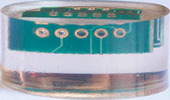
The cross sections expose a selection of the holes, or vias, in the board. The holes are where drilling exerts thermal and mechanical stress on the materials that make up the PCBs. They are therefore the most likely place for critical faults to occur.
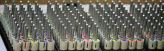
The manufacturing of PCBs is a series of high-temperature and -pressure processes required to bond the various layers of the board together. There are also several delicately balanced chemical processes that create the correct levels of conductivity and solderability required for when the boards are fitted to their end products. Once the boards come off the line, they are subject to further mechanical and heat stress when the panels are scored and the vias are drilled. Most of the drilling is done by mechanical drills (Figure 2) as opposed to lasers.
When the boards are incorporated into the machinery or product for which they were designed, they go through several processes where temperatures exceed 260°C.
Why a zero defect policy is non-negotiable
Any latent or undetected defects in the boards will most probably manifest in the form of dud products or, worse still, result in product failure in the field. With domestic products, this may be annoying, but it is unlikely to be harmful. With professional equipment in the automotive, medical or military markets, it could well prove to be fatal.
Microsectioning is a form of quality control designed to reveal faults and to expose potential weak spots that could result in product failure.
The last great check
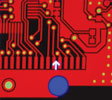
During the manufacturing process, each layer of every PCB is optically checked on automatic optical inspection (AOI) equipment (Figure 3). Once the boards are assembled, they are electrically tested (Figure 4) to ensure that the tracks are conducting current correctly. However, these tests cannot show areas that have the potential to fail or details that might cause problems in later assembly processes.
Microsectioning enables technicians to literally look inside the PCBs after they have been through the rigours of laminating, drilling and scouring to inspect the substrate bonding, through-hole plating and the copper layers that form the tracks.
The resin and metal layers that make up a typical PCB are designed to withstand particular levels of heat and mechanical stress. There are certain processes in the manufacture of the boards that can exceed these levels if everything is not kept within strict parameters. Bearing in mind that the laminations are extremely thin, their tolerances are very small, so faults that are only microns in size will cause the board to fail.
The main culprit
The drilling process is at the centre of just about all the faults detected by microsectioning. This is because the spindle speed is critically associated with the rate of drill bit entry and exit. Bad co-ordination of these two factors will cause excessive heat build up. If the resin laminate melts, the copper tracks will be compromised and smearing will adversely affect solderability and conductivity.
The drilling process will also cause problems if the drill bits are slightly blunt, chipped or clogged.
The accomplices
Also on the wanted list are under-cured resin substrates which do not have the required thermal performance, sub-standard entry and exit materials and sub-standard lamination and chemical processes. In some cases, faults may seem to be caused by the drilling process, but will in fact be due to drilling into inferior substrate. Microsectioning technicians must be able to spot the different causes and know when they are dealing with a problem caused by a combination of factors.
The Devil’s details
The following are nine of the most common faults detected by microsectioning.
1. Nail-heading
This fault comes in several different forms, all associated with the drilling process. Essentially, nail-heading involves the distortion of the copper inner layer and gets its name from its shape, which resembles a nail head.
The most common cause of nail-heading is thermo-mechanical distortion and is usually associated with small diameter holes. When drilling is performed incorrectly, the resin layers holding the copper tracks in place are softened. This is a direct result of excessive spindle speed or of the drill bit being held in one position for too long. Once the resin substrate is compromised, it starts to release the copper layer. The entry and exit motion of the drill bit pushes and pulls the copper and forms the nail heads at each end of the hole being drilled. Mechanical nail-heading causes unidirectional distortion and is usually accompanied by a heavy resin smear over the copper.
Nail-heading is more likely to occur in PCBs with higher numbers of layers and occurs when one or more of the following factors arise: the resins in the substrate are under-cured; poor entry and exit materials are used; the drill bit is clogged; the spindle speed is too high and the rate of entry and exit of the drill bit is incorrect.
2. Smear
There is always a certain amount of resin smear on hole walls and this is removed with de-smearing techniques, but these methods are not sufficient to remove excessive smearing which is what we are talking about here.
The main causes of smear are: under-cured resin; the drill being inserted into the PCB too often; excessive spindle speed; the drill being inserted into the board too slowly which allows the drill to build up heat; under-cured resin in exit material; blunt or chipped drill bits; and incorrect smear removal process.
There are two types of smear: nail-heading and thermo-mechanical. Nail-heading smear is the result of resin, melted by incorrect drilling procedure, being deposited at the openings of the hole and forming doughnut shapes. The resin is usually the same colour as the resin used in the substrate of the board. Thermo-mechanical smear is caused by build up of excessive heat in the hole during drilling. The resin in the board melts and coats the walls of the hole with a heavy, clear layer. This effectively insulates the copper tracks.
Smearing prevents the proper plating of the hole walls which, when it comes to populating the board with microelectronic components, will cause the soldering function to fail.
3. Resin fracturing or haloing
Surface fractures occur on the outer surfaces of the board, around the entrance of the holes. Hole wall fractures of the resin layers occur inside the board between the conductor layers. Surface fractures can be detected without the use of microsectioning, while hole wall fractures are only visible with microsectioning.
Surface fractures occur when the drill enters the material too quickly, or when substandard entry material is used. If the entry material is too soft or too thin, it will not support the drill as it enters the board. The drill then forms a burr on the top of the panel which separates the base copper foil from the resin substrate, causing a crack in the resin.
Hole wall fractures arise when the drill speed is too high and the drill enters the board too slowly. The problem is exacerbated by under-cured resin in the board and the use of inferior entry and exit materials which clog the drill flutes.
4. Gouging
This fault is characterised by the excessive and irregular removal of base material from the hole walls. It occurs in the resin and glass reinforced layers.
The usual drill problems of chipped bits, clogged flutes and incorrect speed to entry ratios can cause gouging, but the more probable cause is overly aggressive de-smearing or glass etching processes.
5. Copper pad tear-out.
The integrity of a PCB depends on many factors. If the resins used do not cure properly, or if they are compromised during the manufacturing process, the board might start coming apart when drilling, scouring and etching processes take place.
Copper pad tear-out occurs when the copper layers are dislodged from the base material during the drilling process. The usual cause of this is excessive heat during the drilling process or failure of incorrectly cured resin. In the absence of these two factors, incorrect hole to pad ratio will cause it. This is where the design has called for holes to be drilled too close to each other, leaving an insufficient amount of base material between them.
6. Wedge voids
These are characterised by a wedge-shaped ring of resin missing around the hole wall where the resin and copper layers interface. Where this occurs, there are also sections of copper missing or folds in the copper plate.
The root causes of wedge voids lie in the lamination pressing or sandwiching process when the PCBs are layered and assembled. At this stage, incorrect process control in the oxide process and deficient prepreg resin flow and incorrect resin cure are the culprits.
7. Pink ring
This fault has a similar appearance to wedge voiding as it occurs in the same area – around the circumference of the hole, between the copper and resin layers. But that is where the similarities end.
Pink ring is the delamination of the inner copper layers from the resin layers caused by the failure of the bond between the prepreg layer and the copper oxide surfaces. The failure is triggered by acid attacking the oxide surface through micro delaminations. The delaminations are a result of weak bonding which is then aggravated by normal drilling. So, it is not a drilling related problem, but is often attributed to drilling because it typically appears in areas around drilled holes, but can also arise in areas away from holes.
Essentially, pink ring failure is set up by these control deficiencies: lack of process control in the oxide process; incorrect heat-up rate during lamination; prepreg with low surface resin; and faulty etch-back processing.
8. Burrs
These are entirely drill related, but are due largely to failures in quality control.
Burrs cause distortion of the outer copper layers on both sides of the PCB at the hole openings.
The main causes are: entry and exit material being too thin for drill speeds and feeds; debris trapped between the panel and the entry or exit material; the opening in the drill spindle pressure foot being too large, allowing a vacuum to develop which then lifts the entry material; the use of entry material which is too soft.
9. Misregistration
Misregistration happens when the holes drilled miss their intended copper tracks either inside or on the outside of the PCB. It can happen that all but one of the tracks is correctly positioned, but, as they say: ‘A miss is as good as a mile’ – the board will fail.
When individual layers do not align correctly the cause could be: incorrectly punched photo-tools; misalignment during photo-imaging; material movement during etching or lamination. Where the drill missed all the layers, the cause is probably the misalignment of tooling holes on the drill table in relation to the panel tooling holes; the drill machine incorrectly positioned; a drill bit with excessive run-out; or deflection of the bit on entry.
The beginning defines the quality of the end result
Experienced PCB design engineers know that their task is as much about accommodating the rigours of manufacturing as it is about end use. Tightly controlled PCB manufacturing processes are critical to the long-term stability of the end product. Because of this, communication between the client and the manufacturer is essential. The designer and the manufacturer must be on the same page when it comes to the assembly process that the PCB will be put through when it is incorporated into the final product.
RoHS compliance raises its own issues where glass transitional profiles, Z-axis CTE, dielectric constants and points of dielectric breakdown must all be considered prior to manufacture. As a guide, designers should adhere to IPC 4104/124 requirements and communicate the exact results they are expecting from the manufacturer since details such as resin flow, gel time and various other factors all combine to produce specific results.
| Tel: | +27 21 700 4900 |
| Email: | [email protected] |
| www: | www.cirtech-electronics.com |
| Articles: | More information and articles about Cirtech Electronics |


© Technews Publishing (Pty) Ltd | All Rights Reserved
 printer friendly version