


An ever increasing number of electronic functions are being squeezed into smaller and smaller products – whether it’s consumer electronics, computers, automotive or medical technology, the overall trend is reduction in size. This manifests as not only smaller finished products, but also shrinking components. It all adds up to printed circuit board (PCB) assemblies becoming more densely packed and using smaller features.
Chris Nuttall, chief operating officer at NCAB Group, takes up mobile phones as an example. “Just consider the way they have evolved,” he poses.” A modern phone is not just a phone, it’s a smartphone. It’s so much thinner, lighter and smaller than the mobiles we had 20 years ago, but in terms of what it can do, it is light years more advanced than its predecessors.”
As a consequence, the PCBs inside are having to accommodate more and more functions, making the design itself much more complex, and all of this on ever smaller circuit boards. To put numbers to this evolutionary process, Nuttall compares a modern camera made by NCAB customer, Hasselblad, with an older model: “The Hasselblad H1D, which was released in 2002, could deliver images with resolutions of up to 22 megapixels,” he explains. “The images produced by Hasselblad’s latest model, the H5D, can have resolutions of up to 200 megapixels.”
The sensors, memory and processors at the core of this new and vastly more advanced technology obviously demands a much more complex PCB at its heart. The onset of these increasingly sophisticated electronic products has led to more advanced PCBs becoming more commonplace.
The specifications for advanced electronics require so-called HDI (High Density Interconnect) solutions with greater number of layers, more connections both on the surface and inside the PCB, utilising finer conductor widths and narrower spaces between them.
This leads to a design that is based upon smaller, laser-drilled microvias (blind vias), since normal through-hole vias simply would not fit into the space available. For this reason manufacturers are producing more boards that also incorporate buried vias, which increases the number of interconnections within the board and frees up valuable space on the outer layer for more components to be placed.
The increased number of layers, together with the use of micro via technology, also requires the use of thinner prepegs and cores than in conventionally manufactured boards, which also leads to increased demands upon the factories.
More production stages
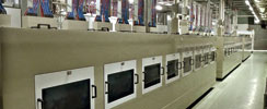
According to NCAB Group Sweden’s technical manager, Kenneth Jonsson, widespread miniaturisation is putting far greater demands on the production equipment at the PCB factories. “Many of the stages in the production of HDI boards are similar to those used for the manufacture of conventional boards,” he says. “However, HDI production calls for considerably more sophisticated equipment in order to achieve the tiny geometries that are required.
“And not only does incorporating several layers of buried vias and/or micro vias into the boards require a number of additional steps, but these also need to be repeated several times and all of that increases the degree of complexity and the risk of error,” he continues. “All the geometries are much smaller on HDI boards, which calls for better dedicated equipment designed for high-tech manufacturing. Many factories do have laser drills, but there aren’t, unfortunately, as many who also possess the appropriate plating equipment and processing experience to enable them to actually make good-quality, reliable HDI boards. That’s why NCAB puts a great deal of time and effort into qualifying and verifying a factory before giving it our seal of approval to manufacture HDI boards for our customers.”
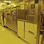
The first consideration in generating micro vias is the requirement of advanced laser drills that can drill blind holes down to 50 μm, although most micro vias normally have a diameter of around 100 μm. The latest generations of these machines are capable of drilling up to 500 holes a second.
Following on from that, the transferring of the circuit pattern onto an HDI board is an equally critical operation that calls for the highest precision, which the traditional photography based techniques cannot achieve, according to Jonsson. Instead, HDI board makers either use CCD camera aligned imaging machines with parallel lighting, or Laser Direct Imaging (LDI) systems, which images the pattern directly onto the bonded photo-imagable material. This makes for improved quality as no photo tool film is used, thus enabling a much greater accuracy of transfer of pattern features down to 50 μm.
The right equipment and clean rooms
To ensure the best possible result in the imaging transfer process, Jonsson says it is vital that it be performed in special clean rooms with carefully controlled temperature and humidity levels. The clean rooms used for these processes meet the US FED STD 209E 10,000 class. This class has constituted the industry standard for many years now and stipulates that the concentration of airborne particles 0,5 μm in size should not exceed 10 000 particles per cubic foot.
“Today the best factories have clean rooms that meet the class 1000 requirements,” Jonsson says. “To give another idea of what this means; the air in our normal everyday environment contain 1 million particles, of the same size, per cubic foot. However, good quality clean rooms are expensive, both to buy and to properly maintain.”
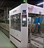
Producing HDI boards also requires a different type of plating line. For non-HDI boards, manufacturers can usually make do with ordinary plating lines with vertically held panels that use mechanical and air agitation, allowing them to get the plating chemicals to facilitate good copper plating onto the surfaces and into the holes (the through-hole part of the plating requires good solution flow within the holes to obtain a reliable or uniform plating thickness).
However, the method described above is not really suitable for HDI boards with blind holes that can measure 100 μm or less in diameter, therefore most factories use horizontal plating lines as well as Vertical Continuous Plating (VCP) lines. These methods involve spraying the plating chemicals onto the pads under high pressure, which ensures that the micro vias are properly plated.
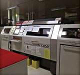
Positioning the solder mask correctly against the pattern poses a significant challenge, since extreme components such as 01005 and μBGA circuits with 400 μm or finer pitches have to provide registration down to 37 μm, or in extreme cases down to 25 μm. To achieve this, CCD exposure units are required.
PCB makers now have the possibility to use special LDI units to expose the solder mask, as the solder mask manufacturers have developed special solder mask inks that require lower energy to polymerise, in order to support HDI designs.
Looking under the bonnet
Nuttall explains that the NCAB Group has to carry out a thorough examination of all aspects of a factory’s production processes and equipment when assessing whether or not it meets the demands for high-tech manufacturing. As he puts it, “it’s like looking under the bonnet and servicing the car before buying it.
“If a factory says that it has laser drills, and is therefore capable of producing reliable high-tech PCBs, it’s rather like saying that all you need to do in order to become a new Michelangelo is to get yourself a hammer and chisel. We know that laser drilling equipment is not the start and finish when it comes to HDI production – it’s equally important to have the right kind of plating equipment, to have the right chemistry as well as knowing how to handle, control and verify the full plating process.
“We also look at what kind of chemicals and methods they’re using, image transfer equipment and procedures, and this is in conjunction with understanding the numbers behind the factory’s real experience in this field and their performance – both of which are crucial factors.”
“Since we are looking for our factories to specialise in manufacturing advanced boards, it has to be a key part of their core activity,” adds Jonsson. Currently there are 11 factories across China and Europe which are able to manufacture HDI PCBs for NCAB’s customers.
Nuttall adds that it is important for NCAB to listen to its customers, and work to understand the details of their designs and their requirements. “We find the right factory for each specific project, depending on its complexity, volumes and any other specific demands,” he explains. “And our strategy to ensure that we maintain and develop a best in class and secure factory base, continues within this field of technology as we always have more than one approved source that can support NCAB and our customers.”
Jonsson emphasises the importance of the factory being able to not only manufacture advanced PCBs, but also keep the number of production errors to a minimum. “Take HDI boards as an example,” he says. “Producing this type of board according to the 3-4b-3 method involves laminating, drilling and plating it four times. If they return a 10% rate of failure during each round in the factory, the number of boards they would end up scrapping would exceed the volumes they actually deliver. In such a case you need to question the quality of the items that make it through to the delivery stage.
“When you consider that the components on the board can cost more than 100 times the board itself, it’s imperative you can rely on the quality of the board. Otherwise, it can be incredibly expensive, if you’re forced to scrap the product at a later stage.”
Get the design right from the start
Yet another aspect that must be prioritised when it comes to advanced boards is the design itself. The margins are tiny with regard to such factors as conductor widths, isolation distances between copper features, impedance requirements, hole sizes and their relation to capture and target lands. All this poses a considerable challenge at the layout stage.
The design rules should be realistic and adapted to volume production right from the start, warns Jonsson, adding that there are a number of pitfalls when only considering prototype factory design rules. “One example may be making the inner layer cores too thin so as to produce a good capacitive coupling. It might work in a prototype factory, where great care is taken to basically hand-process these thin inner layer cores; however it could lead to major problems when the product is in volume production, since they may have different capabilities and in this instance the thinner cores may easily get stuck during processing through long, volume oriented etching lines since they are basically too flimsy,” he explains. “We thus recommend that one avoids, if possible, inner layer cores that are thinner than 75 μm as our experience tells us that this design guideline works well across our higher-technology factory base.”
Jonsson adds that, if there is enough space on the board and the component is available with different pitches, it is recommended to select a component with a larger pitch since it reduces the complexity of the board and saves costs. “Smaller components may be less expensive to purchase or more readily available, but this approach might render the board unnecessarily expensive in relation to its end application,” he points out. “Opting for small components usually increases the complexity of the circuitry, and therefore the board will increase in cost also.
“This is where the customer should work with NCAB to determine if the design needed for such components is a cost effective one – is the reduced cost associated with buying more readily available, but more complex, components balanced with a potentially more expensive PCB? If, for example, it is to be used in mobile phones destined for the consumer market, or in low-volume production.”
With the advent of more PoP (Package on Package) type components being used in the industry, Jonsson also advises customers to check whether the assembly house is familiar with the technology and the extra costs it might involve. “Of course, smaller components are space saving, which could produce a cheaper board, as long as it doesn’t mean making it more complex, with several levels of micro vias or adding buried structures etc. One invariably has to weigh up the space contra complexity issues at the design phase,” he states.
“NCAB makes a point of being involved right at the very start in order to help customers find the right solution. One has to realise that there are real differences between producing prototypes and volume production, explains Jonsson: “If you focus on the wrong things from the start, it could jeopardise the entire project if you find that your design can’t be applied in volume production. My recommendation is to initiate a ‘seamless project’ together with us at an early stage; in order to ensure that the board can be manufactured at a reasonable cost with the right level of complexity for the design and also for reliable yields.”
“The advantages of turning to NCAB Group is that we possess the skills and knowledge both on the design and manufacturing sides. We know what the factories need in order to successfully deliver quality products, within realistic lead times. We know which factories are best at fulfilling different types of requirements, and we also know how to design boards that will give customers high yields and best in class quality end products,” concludes Nuttall.
For more information contact Nechan Naicker, Cirtech EDA, +27 (0)12 665 0375, [email protected], www.cirtech-eda.com
| Tel: | +27 21 700 4900 |
| Email: | [email protected] |
| www: | www.cirtech-electronics.com |
| Articles: | More information and articles about Cirtech Electronics |


© Technews Publishing (Pty) Ltd | All Rights Reserved
 printer friendly version