


PCB designers today are dealing with an array of new challenges, including greater electronic and mechanical design complexity, tighter constraints and rules, and the need to stay on top of a fast-changing supply chain.
These and other emerging issues can cause extra design spins that drive up engineering costs and delay product introductions, ultimately costing money.
Leading-edge PCB design tools are helping to address these concerns by providing up-front design intelligence that addresses these and other areas of the design process. Rules and constraints can be established earlier in the design process, reducing the need for potentially expensive changes late in the design process.
Electrical design is becoming more integrated with mechanical design so that, for example, changes can be pushed from the mechanical computer aided design (MCAD) environment to the electrical computer aided design (ECAD) environment, and vice versa. Finally, embedded component management systems are keeping designers up to date on availability, delivery and pricing.
PCB design challenges
Today’s electronic products deliver more functionality than ever before, so engineers are tasked with designing products with more PCBs, more layers and more components. Enclosures are shrinking and taking on more aerodynamic shapes which makes it more critical than ever for PCB design to take into account the shape of the enclosure. Likewise, the physical aspects of the internal electronics are becoming more important than ever to the mechanical design.
The increasing speed and functionality of the latest cutting edge products, combined with their smaller size, makes it more difficult than ever to avoid power integrity, thermal integrity and signal integrity problems. Dealing with the supply chain has also become more complicated than ever before: it is no longer possible to specify a particular component at the beginning of the design process and assume that it will still be available at the manufacturing stage. Designers need to continuously monitor changes in the supply chain and be ready to react to changes by substituting different components.
PCB design tools expand beyond automatic routing
Component placement and routing were the original capabilities offered by PCB design tools and are still vital to today’s designers. Modern leading-edge design tools help maximise routing efficiency and flexibility with interactive routing that lays route sections along the cursor path, enables pushing or walking around obstacles and automatically follows existing connections.
Cursor guided routing makes complex manual routing around obstacles fast, easy and intuitive. The user creates the path of the route with their mouse and the interactive router attempts to place the tracks according to that path.
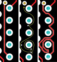
Figure 1 illustrates how complex routes can be created quickly with the routing path guided by cursor movement. The left image shows a normal, minimal length route, the centre image indicates the cursor path, with stars indicating where clicks were made to commit sections of the route. The right image is the resultant routing. Although an extreme example, this shows how few routing commits are required to place many tracks.
Component placement is another area where substantial improvements have been realised in the latest PCB design systems. For example, many will have experienced wasted time trying to hunt down a component on their board layout, only to find that it was in a completely different location relative to the schematic design. Cross-select component placement saves time by making it possible to select specific components on the schematic in a specific order and then place those components on the board layout in the order they were selected. This helps to keep designs closely aligned and organised, and easy to edit in the future.
Establishing rules and constraints earlier in design process
As functionality, power dissipation and signal speed increase, while enclosures shrink, design rules are becoming tighter and more difficult to manage. New PCB design software is helping to address this challenge by enabling designers to set up rules and constraints earlier in the design process in order to ensure the logical and physical integrity of the design and minimise the need for changes later on.
Checks against any or all enabled design rules can be run in real-time as the designer works, as a batch check with results listed in the messages panel or within a generated report. This feature should be used on every routed board to confirm that minimum clearance rules have been maintained and that there are no other design violations.
Defining, managing and documenting the layer stack has also become a much more critical issue with the increase in the number of layers in typical PCBs. This challenge is increased by the advent of flexible PCBs comprised of a series of rigid and flexible layers that can be folded to fit into unusually shaped enclosures. These copper layers are defined in the design environment along with layers of insulation material that separate them.
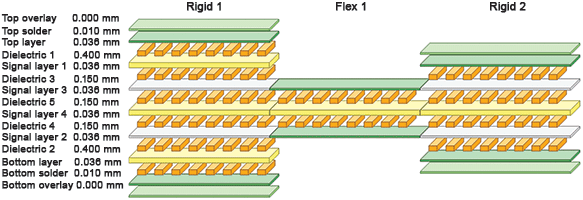
New layer stack management tools are being developed to create multiple layer stacks within a single PCB design, simplifying the task of defining a rigid-flex PCB. The first step is defining the overall shape of the PCB. Next, the designer defines a master set of layers, including all layers needed in the rigid-flex design. The designer has the ability to define multiple layer stacks where each stack includes only the layers needed for each of the rigid and flexible zones of the PCB. Different rigid and flexible zones are established where each sub-stack is applied. Finally, the designer generates the detailed output fabrication and documentation files needed to fabricate the rigid-flex PCB.
Mechanical integration beyond interchangeable file formats
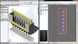
Packaging and electronic assemblies are becoming more tightly integrated than ever before due to increasing design complexity and reductions in enclosure size. The manual import and export of neutral file formats is limited by the time consuming nature of this process as well as the potential for data loss that can occur when 3D MCAD data is moved into a 2D PCB design environment. Cutting-edge PCB design systems address this challenge by automating the process of pushing changes to component placement, board shape, mounting holes, etc. between the MCAD and ECAD environments.
A detailed comment and revision history shows exactly what changes were made to the design and both MCAD and ECAD designers have the ability to accept or reject changes. Board assemblies can be exported to the mechanical designer’s environment with included copper geometries so that detailed thermal, vibration and other simulations can be performed.
Overcoming part selection difficulties
When passing by the desk of an electronic engineer, one is likely to find a stack of catalogues of components from favourite suppliers. The catalogues are usually well-worn because the engineer consults them on a regular basis to search for necessary circuit components and answer questions such as: What parts are available? What functionality do they offer? What are their specs? How much do they cost? How quickly can they be delivered?
The problem with this approach is that a lot of time is spent paging through catalogues and frequently the data in the catalogues turns out to be outdated. The worst case scenario is that the problem is not discovered until late in the design cycle and ends up affecting the product delivery schedule.
The most advanced PCB design systems can help overcome this problem through direct connections to supplier web services, making it possible to search across the supplier’s online product catalogue in order to ensure that the information generated in the search is current. This live data – parametric information, data sheet links, pricing and stock information, etc. – can be instantly incorporated into the design, saving the time that would otherwise be required for manual data entry.
A live link can be incorporated in the design so that the information will automatically be updated when a change is made to the supplier’s online catalogue. Designers can also choose to be notified when such changes are made so they can take action to avoid disruptions to the supply chain.
Designers can also specify alternative part choices in order to maximise their flexibility to respond to a dynamic supply environment. The primary and alternative part choices will automatically be swapped if a primary component becomes unavailable or incompatible through a specifications change.
| Tel: | +27 12 665 0375 |
| Email: | sales@edatech.co.za |
| www: | www.edatech.co.za |
| Articles: | More information and articles about EDA Technologies |


© Technews Publishing (Pty) Ltd | All Rights Reserved
 printer friendly version