
Board profiling for production versus rework
If we consider profiling a PCB (printed circuit board) for reflow in production, we are generally concerned with achieving an even delta-T (ΔT) across all of the joints being soldered. This is accomplished by evenly heating both the top and bottom sides of the whole board, generally through a multi-zoned convection reflow oven. The capacity of the oven would be appropriate to the size or thermal mass of the PCB and the production throughput requirements.
When we consider reworking an array package such as a BGA (ball grid array) or CSP (chip-scale package), it is recognised that process control is of paramount importance to achieve a successful result.
The normal way to approach the rework is to try and emulate the production reflow profile for the individual component being removed or replaced. The nature of the operation dictates that we only wish to reflow the component being reworked and therefore we have to heat a specific area of the circuit board. Selective heating of an area of board can inadvertently cause process failure even when all the parameters appear to be correct. This article discusses the influential factors and the potential pitfalls to be avoided.
Process yield problems
In some cases, particularly on larger PCB assemblies, failure may still occur, giving low yields when all of the conditions for rework are apparently correct. The requirements for a solder profile are generally well understood; they are normally dependent on the materials being used (solder paste or flux) and would typically be as shown in Table 1.

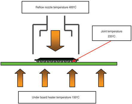
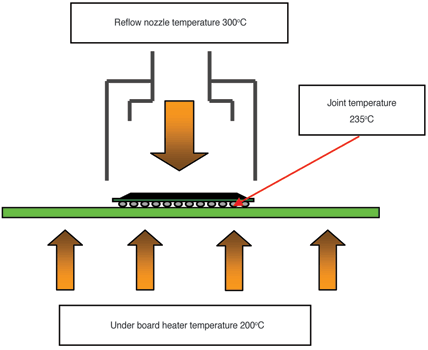
On any reflow soldering system that heats both sides of the PCB assembly, the required solder joint temperature is a function of how much heat is applied to both the top and bottom sides. It is quite possible to achieve the same solder joint temperature with a number of heat settings. The two examples shown in Figure 1 illustrate this.
Practical case study
The graph in Figure 2 shows a trace of a profile taken from under a 492 PBGA (plastic BGA) on a PC motherboard where the thermocouple trace appears to be normal – hitting the desired pre-heat, soak and reflow temperatures. In this case with either solder paste or flux, a very low pass rate was achieved.
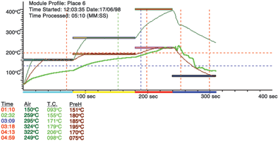
The graph in Figure 3 is the final profile that was used, and as shown, the two traces are very similar but the heating has been done in a totally different way. In this case, the number of zones has been increased to four, reduced the top air temperature significantly while increasing the underboard heat to the whole board and utilising an underboard centralised heating zone.
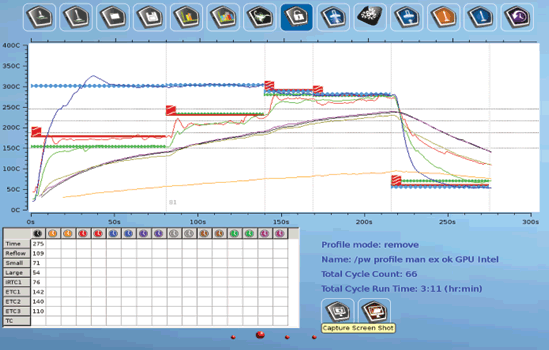
The reason behind the yield problems was due to the plastic BGA warping during reflow, caused by excessive source temperature on the topside of the PCB.
The following is an explanation of the kind of faults that can occur when yields are low despite everything appearing to be set correctly (ie, perfect screen print, no board damage, and accurate placement).
Warpage
A major cause of defects is when either the PCB or the component warp during reflow. Even minor deformation can lead to defects, such as open solder joints and solder shorts. A normal PBGA stands off the PCB by about 20 mil (20 thousandths of an inch) and lifting by even 5 mil across the device is enough to cause an open circuit.
Another factor is that the larger the device, the more prone it will be to these problems. Even if the board or component survives the process with no apparent defect, the joint will be under constant strain as the board returns to its normal shape – causing long-term reliability problems.
Figure 4 shows unsoldered joints caused by PCB warpage; this can also be caused by component warpage. The joints in the centre of the component have lifted above the PCB and were not able to make the solder connection. This is more typical when using only flux dip as there is no solder paste to make up the void area. Another characteristic is that the opens will generally be towards the centre of the device.
Figure 5 shows solder shorts; in this case the deformation has caused the solder paste and the solder balls to combine into solder shorts. This is more typical with solder paste, and is normally characterised by shorts on the device periphery, especially in the corners when the device becomes ‘dog eared’ during reflow.
The solution to the problem of warpage is generally related to the profile settings, particularly insufficient underboard pre-heat temperature combined with too high a top temperature. A board that exhibits poor thermal balancing can also lead to problems.
On large PCBs underboard support can also be a factor, with the PCB sagging under its own weight. Downward pressure should not be applied by either the reflow head or vacuum, as this will exacerbate any problems.
Component delamination
Another cause of solder shorts is delamination of the component substrate during reflow. Plastic packages are generally hydroscopic, meaning that they absorb moisture during exposure to the atmosphere. If the device is then rapidly heated, the moisture expands to create a cavity inside the device. This effect is known as ‘pop-corning’.
This defect is characterised by a blister on the underside of the component due to the internal expansion. Under X-ray inspection, one would normally see solder shorts towards the centre of the device. Figure 6 illustrates this effect.
The solution to this problem is to slowly pre-bake the components and boards prior to reworking them. This will allow any moisture to escape slowly. Some companies already specify this as a prerequisite before any rework is carried out. Users should also ensure that only correctly stored devices are used for both assembly and rework (components are generally supplied in a dry pack that should be re-sealed after opening).
Faults caused by non-simultaneous reflow
The reason that manufacturers strive to attain simultaneous reflow is that having a large ΔT across a component can lead to rework and production defects.
Some factors can be directly influenced by the profile settings while others are determined by the physical makeup of the PCB assembly.
The first factor that will influence how ‘simultaneous’ the reflow is, will be profile temperatures at the point of reflow. More specifically, how quickly the solder passes from solid to liquid state.
Example: reflow input temperature too low
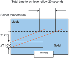
Figure 7 shows a graph section of a component’s solder joints going from solid to liquid at a melting temperature of 217°C. Assume that the achieved ΔT across the component is 10°C.
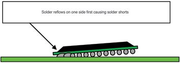
The rate of temperature rise (ramp rate) will determine the duration of reflow from start to finish. This is directly proportional to the input temperatures set on the profile; in this case the ramp rate is 0,5°C per second. The type of problem this profile is likely to cause is shown in Figure 8.
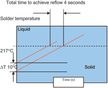
The solution would involve changing the profile input temperatures to achieve a higher ramp rate. This would in turn produce a more simultaneous reflow as illustrated in Figure 9.
Factors that influence ΔT
There are other factors that will influence ΔT on any PCB assembly and these are often out of the control of the rework machine manufacturer. The position of the component on the PCB is a major influence – if a component is placed at the edge of a board, the temperature of the outer two sides will generally be greater than the temperature of the inner sides. This is due to greater heat dissipation towards the centre of the PCB.
Another factor is the area to which some solder balls are connected. It is quite common on a BGA for a centre array of solder balls to be connected to a ground plane specifically to dissipate heat from the component die. These balls may require extra time to reflow.
Conclusion
Profiling for rework is not always as straightforward as it may seem, and it is important to deliver the correct amount of heat to create a successful profile. Knowing and understanding the potential defects will enable you to achieve consistently high yields.
| Tel: | +27 11 704 6677 |
| Email: | [email protected] |
| www: | www.testandrework.co.za |
| Articles: | More information and articles about Test & Rework Solutions |
© Technews Publishing (Pty) Ltd | All Rights Reserved