


Editor’s note
This article contains several references to the books ‘Right The First Time, A Practical Handbook on High Speed PCB And System Design, Volumes 1 and 2,’ written by Lee Ritchey and published by Speeding Edge. These books (or digital versions of them) can be purchased online from the website www.speedingedge.com
The question “What is the current carrying capacity of a through-hole via when used to move power into and out of power planes?” comes up when it is time to design the entry of power or current from a DC-to-DC converter into the planes of a PCB or from the power blades of a connector into the planes of a PCB. The question is usually: “How many vias will be needed to ensure there is a good path into the planes?” A further question might be: “How well do these vias perform when used to conduct current into the power pins of a component, such as a BGA, from the power planes?” This article will examine both of these issues.
Vias are cylinders of plated copper that connect from one side of a PCB to the other. When used to conduct power into or out of the planes of a PCB, only the portion of the plated through-hole between the plane in question and the surface is of interest. Figure 1 is a cross section view of a via piercing a PCB.
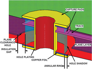
The part of the via that is of interest in this discussion is the plating on the walls of the drilled hole. The current carrying capacity question has two parts. One is the DC resistance and potential heating and voltage drop. The other is the AC resistance or reactance and the
potential voltage drop with a changing current.
Since the question usually refers to the DC voltage drop issue, let’s examine this first.
DC voltage drop and heating in a via
In order to answer the question of currentcarrying capacity of a via, it is necessary to determine its DC resistance. One way to do this is to look at the plating in the hole as a sheet of copper that has been bent into a cylinder. Using this approach, a 12-mil outer diameter (0,33 mm) plated cylinder when unfolded into a flat sheet of copper would be approximately 37 mils (0,94 mm) wide by the length of the via.
Figure 2 is a plot of the resistivity of traces versus length in the three common weights of copper foil.
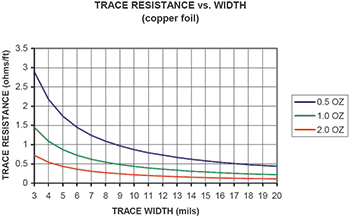
Good PCB fabrication practice calls for a minimum plating thickness of 1 mil (25,4 microns) in a plated through-hole or via. One ounce copper is 1,4 mils (36 microns) thick. Half ounce copper is 0,7 mils (18 microns) thick. Therefore, the plating in the hole is roughly 0,75 ounce copper or midway between one ounce and one half ounce. From Figure 2 it can be seen that a 12” long trace, 18 mils (0,46 mm) wide, has roughly 0,33 Ω of resistance. A trace twice as wide, or 36 mils (0,91 mm), has a resistance of half that or approximately 0,165 Ω.
There are 12 000 mils in 12” (30,5 cm), so the resistivity of our 37 mil (0,94 mm) wide trace is approximately 13,7 μΩ per mil of length. Suppose the length of the via were 100 mils (2,54 mm). Its resistance along its length would be approximately 1,3 mΩ. From this, voltage drop calculations as well as heating calculations can be made.
Suppose the current flow were 3 A. The voltage drop would be 3,9 mV and the power would be 11,7 mW. Clearly, there would be no heating problem at this current level. With a 3,9 mV voltage drop, it is unlikely that this would ever be an issue either. This example presumes that the current must travel along the entire 100 mil length of the via. In reality, the planes are normally midway into the PCB, so only a part of the via is involved resulting in an even smaller voltage drop.
The current flowing in the via must pass into the plane where the plating in the hole meets the copper in the plane. How robust this
connection is depends on how thoroughly the copper edge of the plane has been cleaned after drilling and before plating the copper into the hole. Being a pessimist, I expect that some, perhaps not many, of these holes are imperfectly cleaned. To allow for this reduction in contact area, I have rated my vias at a maximum of 3 A. This is the usual rating for the connector pins in many of the connectors that are used to deliver power into a PCB so it all works out.
A more likely source of significant voltage drop might be in the plane itself. On page 127 of the book ‘Right The First Time, A Practical Handbook on High Speed PCB and System Design, Volume 1’, the method for calculating voltage drops in a power plane is discussed.
Via inductance and AC voltage drop
Current flowing into a PCB from a DC-DC converter is primarily DC or very low in frequency. As a result, the inductance of the via has little effect on this part of the power delivery process. However, current flow out of the planes through the vias into the ICs that consume the energy may have frequency components well into the hundreds of megahertz.
Figure 3 is a plot of via inductance as a function of via length for the most common drill size used with 1 mm pitch BGAs, 12 mils or 0,3 mm. The formula for calculating via inductance is listed on Page 143 of Volume 1. The approximate inductance for a 12 mil drilled and plated via is 35,5 pH per mil of length. This may vary slightly depending on the presence of surface pads and nonfunctional pads but, for this purpose, this value is close enough to illustrate the effect of via inductance on power delivery to a BGA. The inductance is little affected by the thickness of plating which is normally at least 1 mil thick.
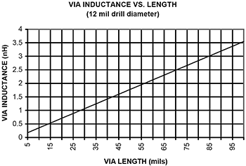
As can be seen from the graph, the inductance gets quite large as the reach down into the PCB to connect with planes grows. This has two adverse effects on power delivery systems.
The first is this inductance adds to the parasitic inductance of the bypass capacitors that are part of the power delivery system (PDS). Even at 15 mils in length, this added inductance is often larger than the parasitic inductance of the capacitors themselves. It is for this reason that choosing ultra-low inductance capacitors, such as IDCs, is not of much help when these capacitors must be connected to planes with vias.
The effect this added inductance has on the performance of a bypass capacitor is to drive its useful frequency lower than might be expected based on the manufacturer’s data sheet. It also raises the Q or quality factor of the capacitor as installed, which increases the height of the
anti-resonance peak when it forms a parallel tuned circuit with the plane capacitance of the PCB. These effects are covered in detail in Chapter 34 of Volume 1.
The second effect is that this via inductance is directly in the path of current drawn from the PDS to charge transmission lines, such as a parallel data or address bus to a DDR memory bank or a PCI bus. Figure 4 illustrates the current flow path for transitions from a logic 0 to a logic 1. As can be seen, the current must flow through the inductance in the total current path which includes the inductance of the bypass capacitors, the inductance of the vias connecting the IC to the VDD plane, the inductance of the ball, the inductance of the IC package, the inductance of the connection between the package and the IC, and the inductance in the power path on the IC itself. Notice that the VSS or ground connection is not involved in this transition.
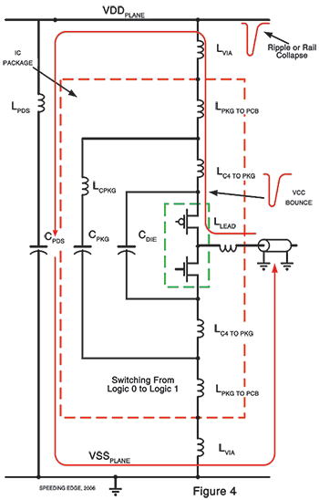
As charge is withdrawn from the capacitance of the PDS, its terminal voltage drops, resulting in what is commonly called ripple or rail collapse. Remedies for excessive ripple are covered in the power delivery sections of Volumes 1 and 2. This rapidly changing current also develops a voltage drop across the inductance between the VDD rail and the VDD terminal of the IC, known as VDD or VCC bounce. This voltage drop or spike drives the VDD rail on the IC negative and, in most cases, drives the entire die and all of the outputs negative as well. This VDD bounce appears as a noise spike on all of the outputs whether they be at a logic 0 or a logic 1. Those at a logic 1 experience a noise spike that can induce a logic failure if the spike is large enough.
The charge drawn from the PDS charges up the parasitic capacitance of the transmission line and the input capacitance of any loads attached to the line from a low voltage to a high voltage.
Figure 5 is an example of VCC or VDD bounce on a quiet output of an FPGA driving a 64-bit data bus. This is a 2,5 V system. The magnitude of the VDD spike is 276 mV or more than 10% of the signal swing – enough to cause logic failures.
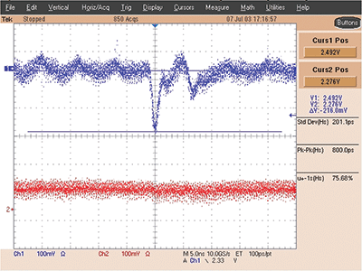
Figure 6 illustrates the current flow path for transitions from a logic 1 to a logic 0. Notice that the PDS is not involved in this transition. The charge put on the transmission line is being removed at this time. The current flow that results develops a voltage drop or spike across the inductances in this path which include the via inductance, the ball inductance, the package inductance and the inductance on the IC.
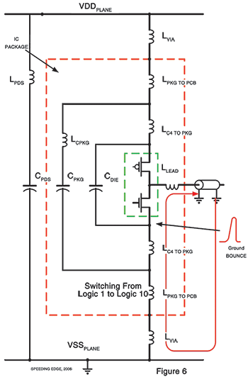
This voltage spike drives the VSS terminal positive with respect to the VSS rail on the PCB. As with the VDD bounce, this voltage spike appears on all of the outputs. Those outputs that are at a logic 0 will experience a noise spike that will erode the logic level and, if large enough, will cause a logic failure.
These VDD and ground bounce spikes are essentially the same amplitude in most CMOS components due to the fact that the power and ground paths into the IC are symmetrical. Either can cause a logic failure. Notice that VDD bounce is accompanied by rail collapse or a negative going voltage spike on the VDD rail. These two noise transients add together to create one large drop in the output voltage of all outputs set at a logic 1.
It is common for systems to fail from this type of noise spike. What makes failures from this mechanism so elusive is that they occur only when all or most of the lines in a wide, parallel bus simultaneously switch from one logic state to another. For a 64-bit wide bus, this is once in 264 times or once in 131 072 times. Systems failing from this source are often described as ‘flaky’.
The equation V = L(di/dt) is used to calculate the voltage drop across an inductance. What can readily be seen is that the magnitude of the voltage rises with increased inductance or increased current and with decreasing time. As IC technologies have migrated down the feature size curve from 250 nm to 130 nm to 90 nm and, as of the publishing of this article, 65 nm, the dt value or switching time of CMOS ICs has dropped dramatically to as little as 200 picoseconds for DDR2 memory outputs.
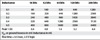
Table 1 illustrates the size of the voltage spike for parallel, single-ended buses with widths from 16 bits to 256 bits wide. This example is typical of DDR buses that commonly operate at 2,5 V. The rise time in this example is 0,5 nanoseconds and was a common rise time for ICs made with the 130 nm process. The total magnitude of the voltage spike is calculated for total inductance in the current path varying from 0,1 nH to
0,5 nH. What can be seen is that the total inductance in the current path must be kept very small as bus widths grow wide and as rise times grow small.
A PCB design engineer has little or no control over the inductance in the IC package other than to exercise care when choosing new components to ensure that the package has been properly designed. The one place where a PCB design engineer can influence the inductance in the current path is the choice of the location of the power layers in the PCB stackup. Clearly, the closer these two layers (power and ground) are to the component side of the PCB, the lower the added parasitic inductance of the power vias will be.
There are many designs that are based on four-layer stackups, with one plane close to the component side of the PCB and the other 40 to 50 mils away at the bottom of the PCB. In such cases, it is not possible to keep both planes close to the IC drawing power from them. Looking at Figure 3, one or the other of the vias will have an inductance of approximately 2 nH. This would suggest that wide parallel memory buses won’t work on four-layer boards.
The PC industry has built hundreds of millions of PC motherboards that are four layers and all of them have large, fast DDR and DDR2 memory systems on them. A fair question might be, “How do they work in view of the forgoing discussions?” The methodology for solving this problem is discussed in another article.
| Tel: | +27 12 665 0375 |
| Email: | [email protected] |
| www: | www.edatech.co.za |
| Articles: | More information and articles about EDA Technologies |


© Technews Publishing (Pty) Ltd | All Rights Reserved
 printer friendly version