News


Samsung is splurging on semiconductors

15 November 2017 News

Market research firm IC Insights’ latest forecast is for semiconductor industry capital spending to climb 35% this year to $90,8 billion, with a large proportion of this coming from Samsung.

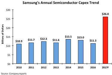
After spending $11,3 billion in semiconductor capex last year, Samsung announced that its 2017 outlays for the semiconductor group are expected to more than double to $26 billion. Bill McClean, president of IC Insights, stated, “In my 37 years of tracking the semiconductor industry, I have never seen such an aggressive ramp of semiconductor capital expenditures. The sheer magnitude of Samsung’s spending this year is unprecedented in the history of the semiconductor industry!”

Figure 1 shows Samsung’s capital spending outlays for its semiconductor group since 2010, the first year the company spent more than $10 billion in capex for the semiconductor segment. After spending $11,3 billion in 2016, the jump in capex expected for this year is unprecedented.

Figure 1.
Figure 1.

To illustrate how forceful its spending plans are, IC Insights anticipates that Samsung’s semiconductor capex of $8,6 billion in 4Q17 will represent 33% of the $26,2 billion in total semiconductor industry capital spending for this quarter. Meanwhile, the company is expected to account for about 16% of worldwide semiconductor sales in 4Q17.

IC Insights estimates that Samsung’s $26 billion in semiconductor outlays this year will be segmented as follows: 3D NAND Flash - $14 billion (including an enormous ramp in capacity at its Pyeongtaek fab); DRAM - $7 billion (for process migration and additional capacity to make up for capacity loss due to migration); foundry/other - $5 billion (for ramping up 10 nm process capacity).

IC Insights believes that Samsung’s massive spending outlays this year will have repercussions far into the future. One of the effects likely to occur is a period of overcapacity in the 3D NAND Flash market. This overcapacity situation will not only be due to Samsung’s huge spending for 3D NAND Flash, but also to its competitors in this market segment (e.g., SK Hynix, Micron, Toshiba, Intel, etc.) responding to the company’s spending surge. At some point, Samsung’s competitors will need to ramp up their capacity or lose market share.

Samsung’s current spending spree is also expected to just about kill any hopes that Chinese companies may have of becoming significant players in the 3D NAND Flash or DRAM markets. This year’s level of spending by Samsung just about guarantees that without some type of joint venture with a large existing memory suppler, new Chinese memory startups stand little chance of competing on the same level as today’s leading suppliers.

For more information visit www.icinsights.com


Share this article:
Share via emailShare via LinkedInPrint this page

Further reading:

From the editor's desk: The art of measuring the truth
Technews Publishing Editor's Choice News
All electronic measurements are a lie. The trick is making the lie as small as possible.

Read more...
TSE has relocated
News
The Technology Station in Electronics (TSE) has entered a new chapter with its relocation from the CSIR campus to TUT-owned building at Ditsela Place in Hatfield.

Read more...
Innovative MyLegrand app
RS South Africa News
Legrand SA is set to launch the MyLegrand mobile application, a digital platform designed to strengthen engagement across its professional network.

Read more...
Kulani Energy acquires critical assets from Optipower
News
Kulani Energy preserves engineering, procurement, and construction capability and positions a wholly women-owned firm at the forefront of South Africa’s grid expansion.

Read more...
From Cape Town to Johannesburg
News
Würth Elektronik South Africa has taken a significant step forward with its recent relocation from Cape Town to Johannesburg, marking a new phase of growth and ambition for the company.

Read more...
Lesley Havenga: Building partnerships for Africa’s electronics future
Editor's Choice News
As Würth Electronik expands its footprint across South Africa and the broader sub-Saharan region, Havenga’s blend of manufacturing expertise, supply chain knowledge, and people-centred leadership appears well suited to the task.

Read more...
Tackling e-waste with help from international partners
News
Every year millions of electrical and electronic devices and appliances, including mobile phones and computers, are thrown away and these items are now the fastest growing waste stream in the world.

Read more...
From the editor's desk: Pricing surge reshapes engineering reality
Technews Publishing News
The recent and continuing surge in memory prices has become more than a supply-chain story confined to global semiconductor markets. We have watched in disbelief as the ASP of memory has risen by over ...

Read more...
Siemens democratises EDA software access
News
This collaboration will provide streamlined access to advanced electronic design automation software for European semiconductor innovation.

Read more...
Components distribution: A promising trend
News
The European electronic components market returned to solid growth in Q1, gaining 16,9%, with broad, but uneven, momentum across the region.

Read more...


While every effort has been made to ensure the accuracy of the information contained herein, the publisher and its agents cannot be held responsible for any errors contained, or any loss incurred as a result. Articles published do not necessarily reflect the views of the publishers. The editor reserves the right to alter or cut copy. Articles submitted are deemed to have been cleared for publication. Advertisements and company contact details are published as provided by the advertiser. Technews Publishing (Pty) Ltd cannot be held responsible for the accuracy or veracity of supplied material.


© Technews Publishing (Pty) Ltd | All Rights Reserved