


To many, the word ‘platform’ has become an overused marketing term. But in the electronics industry, many companies such as Apple, Intel and Cisco Systems have effectively executed platform business strategies to become highly profitable electronics leaders.
In deploying platform strategies, companies make a relatively substantial upfront investment in creating and documenting the blocks they designed for the initial version of their electronics product platform. They then turn those design blocks into intellectual-property (IP) blocks, which they reuse to quickly and easily expand into derivative product lines and models along with next-generation products, delivering each of those derivative products faster and with less effort, less design cost and fewer resources.
Challenges to achieving profitability
Research firm International Business Strategies (IBS) in its 2013 report ‘Factors for Success in System IC Business’ concludes that as the cost of producing an application specific integrated circuit (ASIC) or application specific standard products (ASSP) using the latest silicon processes continues to rise from the 28 nm manufacturing node to 20 nm, 16 nm and 10 nm, companies producing their own chips will increasingly struggle to achieve the traditional end-product revenue goal of ten times their initial R&D investment.
Many make great strides toward achieving this 10x goal by creating multiple derivative products on each node. “Derivative designs can cost 20% of the initial design cost, which means that if a commitment is made to a new product family that has very high development costs, then derivative designs can be implemented at a much lower cost.
“To optimise revenues and profits, it is advantageous for companies to implement multiple [derivative] designs in a technology node,” the report opined. “Implementing only one or two designs in a technology node can result in very high upfront costs and high risks associated with getting good financial returns.
“New design concepts that reduce the cost of implementing new products have the potential to change the structure of the semiconductor industry dramatically,” the report went on.“However, until a new design methodology emerges, semiconductor companies need to adapt their business models to the reality of the changing financial metrics in the semiconductor industry as feature dimensions are reduced.”
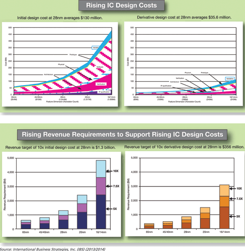
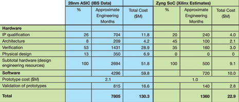
In the study, IBS shows that the design cost of a 28 nm ASIC or ASSP (the first or initial product) is $130 million (Figure 1). Meanwhile, the design cost of a derivative is significantly lower: $35,6 million. Thus, to achieve the 10x revenue goal for both types of devices requires an investment of $1,3 billion for complex devices but only $356 million for derivatives.'
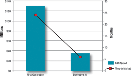
The IBS study shows that companies must spend 650 engineering years to design a complex ASIC at 28 nm. In comparison, a derivative 28 nm ASIC design requires only 169 engineering years to develop, a 3,8x reduction.
Assuming ASIC teams are developing new designs in step with Moore’s Law and are working on a two-year development cycle, it would take 325 engineers to complete a complex 28 nm ASIC in those two years. However, it would take only 85 engineers to complete a derivative 28 nm ASIC in two years; or if a company were to use all 325 of engineers to develop the derivative as well, they could complete the job in six months (Figure 2).
Further, as illustrated in Table 1, if we assume that the initial complex design achieved its 10x revenue payback of $1,3 billion using 325 engineers, a derivative design with a smaller addressable market that is only 80% ($1,04 billion) the revenue size of the initial ASIC’s market would require just 85 engineers over two years to develop a product that would garner a net present value (NPV) that is much better than the NPV of the initial ASIC design. (NPV is defined as the difference between the present value of cash inflows and cash outflows. The concept is used in capital budgeting to analyse the profitability of an investment or project.)
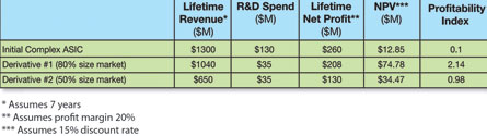
What’s more, the derivative would have a much more favourable profitability index or PI (NPV divided by R&D money spent) than the initial ASIC. Even if that derivative addressed a market half the size ($650 million) of the initial design, it would have an NPV better than the initial ASIC, with essentially the same PI.
Platforms are the best strategy for profitable derivatives
Increasingly semiconductor companies, as well as electronics system companies, are turning to platform strategies as a way to quickly create derivative products and maximise profitability in the face of rising R&D costs, increased competition and customer demand for better everything. Platform strategies further reduce product development time, time to market and engineering-hour costs while simultaneously increasing the profitability of each derivative or next-gen product.
As the IBS study shows, developing derivative designs is a way for companies to ‘optimise revenues and profits.’ And developing multiple derivatives on the same node (in other words, derivatives of derivatives) using a platform approach allows companies to further optimise revenue and profit, as each subsequent design can benefit from lessons learned in the prior design, reuse and a more precise understanding of customer requirements.
Processing choice is key to success of the platform
Two of the biggest business decisions a company can make when deploying a platform strategy are actually vital technical decisions: Which one of the many processing systems will be at the heart of the product platform? And which silicon implementation of that processing system is the best for improving profitability?
In a platform strategy, a processing system must meet or exceed application software and system requirements. It must be scalable and easily extendable; must have a large, established and growing ecosystem, and must allow architects and engineers to leverage prior design work. Finally, it must come from an established, stable supplier with a roadmap and a track record of not deviating from that road map or of issuing endless errata.
While there are candidates that fit some of these qualifications, the one that meets or exceeds all of them is the ARM microprocessor architecture.
ARM has become the de facto standard embedded processing architecture for just about anything that isn’t a PC.
A vast majority of electronics systems today that use advanced embedded processing, from mobile phones to cars to medical equipment, employ ARM processor cores. In particular, the Cortex-A9 architecture is at the heart of many types of systems-on-chip (SoC). It can be found in ASIC designs typically created for the highest-volume, value-added products like bleeding-edge smartphones and tablets, as well as in many ASSP designs for companies wishing to enter established low- to moderate-volume markets that typically compete on pricing for lack of feature differentiation.
To add differentiation to their products, many companies create product platforms that pair an FPGA with an off-the-shelf ASSP based on an ARM processing system. In this configuration, they can differentiate in hardware as well as in software, creating a broader feature set or a higher-performing end product that’s flexible and upgradable – one that helps them outshine competitors offering me-too ASSP implementations that are software programmable only. Adding Xilinx FPGAs to these ASSPs has helped a plethora of companies differentiate their products in the marketplace.
Zynq SoC: the ideal platform solution
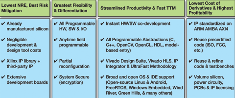
With the Zynq-7000 All Programmable SoC, Xilinx is fielding a platform implementation of the stalwart ARM Cortex-A9 that suits the vast majority of embedded applications. As illustrated in (Table 2), the Zynq SoC offers many advantages over ASIC, ASSP and even ASSP+FPGA combos as a silicon platform.
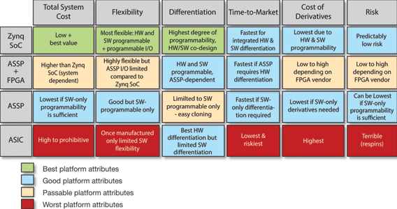
In comparison to other hardware implementations of the ARM processing system, the Zynq SoC has the best feature set in terms of NRE, flexibility, differentiation, productivity/time-to-market, lowest cost of derivatives and best overall risk mitigation (Table 3). What’s more, it has vast cost advantages over other platform implementations – let’s look at the numbers.
The average cost of designing a 28 nm ASIC is $130 million, and thus the 10x revenue goal amounts to $1,3 billion for ASIC designs, according to Barrie Mullins, director of All Programmable SoC product marketing and management at Xilinx. But typical design projects based on the Zynq SoC inherently have a much lower overall design cost and faster time-to-market than ASIC implementations, he believes. That’s because Zynq SoCs supply a predesigned, tested, characterised, verified and manufactured SoC that provides software, hardware, I/O performance and flexibility for differentiation.
What’s more, the Zynq SoC benefits from the fact that Xilinx hardware and software design tools are inexpensive and are highly integrated, whereas ASIC tool flows are complex, have significant interoperability and compatibility issues, and entail complex licensing with costs running in the millions.
Xilinx’s design flow is especially streamlined when designers use Xilinx’s recommended UltraFast methodology. In addition, Mullins says IP qualification costs are low because the Xilinx ecosystem IP is already designed and preverified, while Xilinx tools generate middleware.
As a result, a typical Zynq SoC project runs $23 million. Thus, to achieve the standard 10x revenue goal for design projects requires lifetime revenue of $230 million – a 10x goal that is far more achievable and feasible than the $1,3 billion required to achieve 10x for an ASIC implementation (Table 4).
Using the method described above while analysing the IBS data, if we assume that an initial complex design implemented in a Zynq SoC was able to capture 100% of the same $1,3 billion targeted market, it would require only a $23 million investment using 57 engineers for two years to bring the product to completion.
If we assume that the initial Zynq SoC design has the same 20% profit margin as the initial ASIC design, the initial Zynq SoC design would have an NPV of $107,27 million, with a PI of 3,7, which is dramatically better than the initial ASIC’s NPV of $12,85 million and its PI of 0,1.
The NPV and PI for Zynq SoC derivatives at that same 20% profit margin are even more impressive (Table 5). Xilinx customers have shown that the cost of a derivative in a Zynq SoC platform strategy is typically 60% less than their initial design.
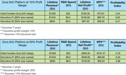
Comparing the Zynq SoC platform derivative at the same 20% profit margin as the ASIC platform derivative addressing a market 80% the size of the initial design, the Zynq SoC platform’s NPV is $96,66 million with a PI of 8,33. This is considerably better than the ASIC derivative, which has an NPV of $74,78 and a PI of 2,14. Similarly, the NPV for the derivative Zynq SoC design addressing a market half the size of the initial Zynq SoC design’s targeted market would be $56,34 million with a PI of 4,86. This is far superior to the ASIC platform derivative’s numbers.
Even if we leave the ASIC platform’s profit margin at 20% and compare the results to a Zynq SoC platform assuming a lower, 15% profit margin (accounting for perhaps higher unit costs for the Zynq SoC), the latter presents a far superior path to maximising profitability. The initial Zynq SoC design at a 15% profit margin would have an NPV of $73,67 million, yielding a PI of 2,45. This is a vast improvement over the initial ASIC’s NPV of $12,85 million and its PI of 0,1 even when the ASIC has 20% profit margin.
For a Zynq SoC platform design that targets a market of 80% ($1,04 billion), the revenue size of the initial Zynq SoC’s targeted market, it would take 23 engineers two years to develop a derivative Zynq SoC-based product. In the end, the product would garner an NPV of $69,78 million with a PI of 6,02. This compares with the ASIC derivative’s NPV of $74,78 million, which is slightly better than the Zynq SoC derivative’s NPV. However, the PI for the Zynq SoC derivative at a 15% profit margin is considerably better than the ASIC derivative’s PI of 2,14, even when the ASIC has a higher (20%) profit margin.
Furthermore, a derivative Zynq SoC design (again at a 15% profit margin) addressing a market half the size of the initial Zynq SoC design’s targeted market would garner an NPV of $39,55 million and a PI of 3,41. That is not only better than the ASIC derivative’s PI of 0,98 but also better than the PI of the initial Zynq SoC.
It should be noted that while profit margins will vary depending on the volume needs of a given market, the data shows that the Zynq SoC is a superior platform choice even for high-volume applications. Even when comparing an ASIC platform at a higher profit margin of 20% to a Zynq SoC platform at a 15% profit margin, the Zynq SoC is a far better platform solution financially as well as technically.
At lower volumes, the Zynq SoC platform is of course even more convincingly the best platform choice to maximise profitability.
Proven platform success with the Zynq SoC
Today, a number of customers in a broad range of application areas are achieving dramatically greater scales of economy by leveraging the Zynq SoC as the heart of their platform strategies. A prime example is a world-renowned maker of high-end electronic control units (ECUs) for the automotive industry, which customer is standardising on the Zynq SoC as a platform solution.
Wielding the Zynq SoC and heavily leveraging the reuse of tightly coupled hardware and software IP, the company has created a highly flexible ECU platform that it can quickly customise for the specific needs of multiple automakers and their different lines, models/configurations and accessory bundles (Figure 3).
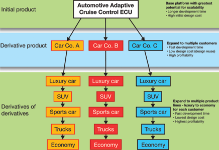
By using the Zynq SoC as a central platform, the company has achieved maximum economy of scale, reducing budgets while increasing the number of products it delivers to a growing number of customers. The upshot is delivering tailored ECUs to customers faster.
For more information contact Erich Nast, Avnet Kopp, +27 (0)11 319 8600, erich.nast@avnet.eu, www.avnet.co.za


© Technews Publishing (Pty) Ltd | All Rights Reserved
 printer friendly version