28 July 2004Manufacturing / Production Technology, Hardware & Services
The European Union has enacted legislation known as the Restriction of certain Hazardous Substances (RoHS) and Waste Electrical and Electronic Equipment (WEEE) Directives.
The EU has set June 2006 as the deadline for electronic equipment suppliers to eliminate most uses of Pb from their products.
With respect to factors such as solderability, ease of manufacture and compatibility with existing assembly methods, pure tin plating is seen by the industry as a potentially simple and cost effective alternative.
However, there is another critical problem out there, and that is - 'tin (Sn) whiskers'.
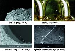
Examples of tin wiskers
What are tin whiskers?
Tin whiskers are electrically conductive, 'hair-like' crystalline structures of tin that may grow from mostly pure tin finished-surfaces. Tin whiskers have been observed to grow to lengths of several millimeters and in rare instances, to lengths of up to 10 mm. Under some electrical/atmospheric conditions, whisker shorts may vaporise into a conductive plasma of metal ions. An arc forms through the plasma that is capable of carrying hundreds of amps with resulting catastrophic damage. Numerous electronic system failures have been attributed to short circuits caused by tin whiskers that bridge closely-spaced circuit elements maintained at different electrical potentials.
Typical characteristics of tin whiskers: growth rate 0,03 to 9 mm/yr; incubation period from days to years; whisker length typically <1 mm and diameter 0,006 µm to 10 µm; electric conductivity in atmosphere, 75 mA max (with whisker dia. 4 µm); in a vacuum whiskers may vaporise into conductive plasma that can carry hundreds of amps; growth mechanism(s) - unknown.
Hi-Q Electronics, local representative for Taiwan Semiconductor, has a presentation available that describes the issue of tin whiskers. Interested readers may contact Stephen Delport, stephen@hi-q.co.za or 021 595 1307.
FineX: Makes shielding clear Avnet Abacus
Manufacturing / Production Technology, Hardware & Services
Panasonic Industry launches high-transparency, low-resistance, flexible transparent conductive film for electromagnetic wave shield with pre-applied OCA.
Read more...Collaboration is now critical RS South Africa
Manufacturing / Production Technology, Hardware & Services
The message emerging from RS Connect is clear: Organisations can no longer rely on internal optimisation alone to secure performance. Competitive advantage is increasingly being determined by the strength of external relationships, shared capability and coordinated action across value chains.
Read more...Disruption is the new normal. Effortless is the new competitive advantage. Seven Labs Technology
Manufacturing / Production Technology, Hardware & Services
Global supply chains have been under pressure for years. The manufacturers still standing are the ones who stopped waiting for normal to return, and started building something better.
Read more...World-first 016008 mm component placement
Manufacturing / Production Technology, Hardware & Services
Fuji has achieved the world’s first placement of 016008 mm (0,16 x 0,08 mm or 006 x 003 inches) size components on printed circuit boards with its SMT pick and place machine, NXTR.
Read more...Lifecycle and obsolescence: Protecting electronics through process Production Logix
Manufacturing / Production Technology, Hardware & Services
At Production Logix, we believe longevity is not accidental. It is engineered through early visibility, structured response, and disciplined execution, in partnership with our OEM customers.
Read more...Maximising squeegee quality and durability Testerion
Manufacturing / Production Technology, Hardware & Services
Transition Automation has announced two new product advancements designed to improve SMT printing performance and extend squeegee life: laser-enhanced Permalex bonding and integrated edge protectors.
Read more...NeoDen ND2 PCB screen printer ZETECH ONE
Manufacturing / Production Technology, Hardware & Services
The NeoDen ND2 PCB screen printing machine is a fully automatic stencil printer designed to deliver precise and consistent solder paste application in modern SMT production environments.
Read more...Understanding the BGA rework process Techmet
Manufacturing / Production Technology, Hardware & Services
BGA rework is a highly technical process that involves removing the faulty component, preparing the circuit board, and installing a new or repaired device, while maintaining the integrity of the printed circuit board.
Read more...Flexible three-process reflow soldering system Truth Electronic Manufacturing
Manufacturing / Production Technology, Hardware & Services
By combining multiple soldering technologies within a single system, the Vision TripleX system enables manufacturers to adapt easily to different assembly requirements, board designs, and production volumes.
Read more...Inline vapour phase soldering for high-volume production MyKay Tronics
Manufacturing / Production Technology, Hardware & Services
The VP2200-100 vacuum inline vapour phase soldering system from ASSCON is designed for fully automated, high-volume electronics manufacturing where process consistency and solder joint quality are critical.
While every effort has been made to ensure the accuracy of the information contained herein, the publisher and its agents cannot be held responsible for any errors contained, or any loss incurred as a result. Articles published do not necessarily reflect the views of the publishers. The editor reserves the right to alter or cut copy. Articles submitted are deemed to have been cleared for publication. Advertisements and company contact details are published as provided by the advertiser. Technews Publishing (Pty) Ltd cannot be held responsible for the accuracy or veracity of supplied material.


 printer friendly version