


Today, most scientists and engineers are using personal computers with expansion buses for laboratory research, industrial control, and test and measurement.
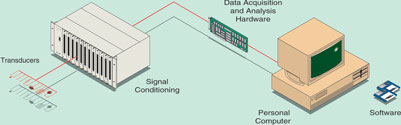
Obtaining proper results from a PC-based DAQ system depends on each of the system elements shown in Figure 1.
Transducers
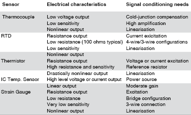
Transducers change physical phenomena into electrical signals. For example, thermocouples, RTDs, thermistors and IC sensors convert temperature into a voltage or resistance. Other examples include strain gauges, flow transducers and pressure transducers, which convert force, rate of flow and pressure to electrical signals. In each case, the electrical signals produced are proportional to the physical parameters they are monitoring.
The thermocouple, for example, combines dissimilar metals to generate voltages that vary with temperature. Thermocouple outputs are very low-level and change only 7 μV to 40 μV for every one degree Celsius change in temperature. Accurate temperature measurements therefore require a signal conditioning system that can amplify the signal with high gain and very little noise or distortion. Thermocouple measurements need cold junction compensation, which corrects for voltages that are formed at the connection of the thermocouple leads to the dissimilar metals.
By sensing the reference temperature of the connection points, compensation hardware or software subtracts out this error voltage from the measured thermocouple voltage. Many signal conditioning accessories include an IC temperature sensor for this purpose.
Other transducers, such as resistance temperature detectors (RTDs), thermistors and strain gauges, respond to changes in temperature or strain with varying electrical resistance. These resistive sensors require an accurate excitation current or voltage source to sense the change in resistance.
Thermistors have a relatively high resistance and can typically be measured with a voltage source and one reference resistor. However, RTDs and strain gauges are low-resistance, low-sensitivity devices that need additional circuitry to enhance their sensitivity and account for lead wire resistance. RTDs are often used in a 4-wire configuration; one pair of wires carries the excitation current and the other pair senses the RTD voltage. This 4-wire configuration avoids errors due to lead resistance because current does not flow in the leads connected to the measurement system. The signal conditioning requirements for these and other common transducers are listed in Table 1.
Signal conditioning
Transducer outputs must often be conditioned to provide signals suitable for the DAQ board. Signal conditioning accessories amplify low-level signals, isolate, filter, excite and bridge complete transducers to produce high-level signals for the DAQ board.
Amplification. The most common type of conditioning is amplification. Low-level thermocouple signals, for example, should be amplified to increase the resolution and reduce noise. For the highest possible accuracy, the signal should be amplified so that the maximum voltage range of the conditioned signal equals the maximum input range of the ADC.
The SCXI front-end signal conditioning system for National Instruments’ DAQ boards has several modules that amplify input signals. The gain is applied to the low-level signals within the SCXI chassis located close to the transducers, sending only high-level signals to the PC and minimising the effects of noise on the readings.
Isolation. Another common application for signal conditioning is to isolate the transducer signals from the computer for safety purposes. The system being monitored may contain high-voltage transients that could damage the computer. An additional reason for needing isolation is to make sure that the readings from the plug-in DAQ board are not affected by differences in ground potentials or common-mode voltages.
When the DAQ board input and the signal being acquired are each referenced to ground, problems occur if there is a potential difference between the two grounds. This difference can lead to a ground loop, which may cause inaccurate representation of the acquired signal, or if too large, may damage the measurement system. Using isolated signal conditioning modules eliminates the ground loop and ensures that the signals are accurately acquired. For example, the SCXI-1120 and SCXI-1121 modules provide isolation that can reject up to 240 Vrms of common-mode voltage.
Filtering. Filtering removes unwanted signals from the signal being measured. A noise filter is used on DC-class signals such as temperature to attenuate higher frequency signals that can reduce the accuracy of your measurement. Many of the SCXI modules have 4 Hz and 10 kHz low pass filters to eliminate noise before the signals are digitised by the DAQ board.
AC-class signals such as vibration often require a different type of filter known as an antialiasing filter. Like the noise filter, the antialiasing filter is also a low pass filter; however, it also has a very steep cutoff rate, so that it almost completely removes all frequency components that are higher than the input bandwidth of the board. If the signals are not removed, they erroneously appear as signals within the input bandwidth of the board. Products designed specifically for AC-class signal measurement, such as the dynamic signal acquisition boards, and the SCXI-1141 module, have built-in antialiasing filters.
Excitation. Signal conditioning also generates excitation for some transducers.
Strain gauges, thermistors, and RTDs, for example, require external voltage or current excitation. Signal conditioning modules for these transducers usually provide these signals. RTD measurements are usually made with a current source that converts the variation in resistance to a measurable voltage. Strain gauges are resistance devices in a wheatstone bridge configuration, which often require bridge completion circuitry and excitation sources. The SCXI-1121 and SCXI-1122 have onboard current and voltage excitation sources that can be used for strain gauges, thermistors or RTDs.
Linearisation. Another common signal conditioning function is linearisation. Many transducers, such as thermocouples, have a nonlinear response to changes in the phenomenon being measured. NI-DAQ and National Instruments application software include linearisation routines for thermocouples, strain gauges and RTDs.
Data acquisition hardware
Basic considerations of analog inputs. The analog input specifications can provide information on both the capabilities and the accuracy of the DAQ product. Basic specifications, which are available on most DAQ products, indicate the number of channels, sampling rate, resolution and input range. The number of analog channel inputs will be specified for both single-ended and differential inputs on boards that have both types of inputs.
Single-ended inputs are all referenced to a common ground point. Non-referenced single-ended inputs are all referenced to AISENSE, not a common ground. The potential at this mode can vary with respect to the system ground. These inputs are typically used when the input signals are high level (1 V), the leads from the signal source to the analog input hardware are short (<5 metres), and all input signals can share a common ground reference. If the signals do not meet these criteria, differential inputs should be used. A differential, or non-referenced, measurement system has neither of its inputs tied to a fixed reference.
An ideal differential measurement system responds only to the potential difference between two terminals – the (+) and (-) inputs. Any voltage measured with respect to the instrumentation amplifier ground present at both amplifier inputs is referred to as a common-mode voltage. The term common-mode voltage range describes the ability of a DAQ board in differential mode to reject the common-mode voltage signal. In differential mode, noise errors are reduced because the common-mode noise picked up by both leads is cancelled out.
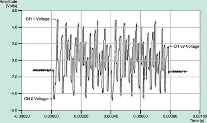
Sampling rate. This parameter specifies how often conversions can take place. A faster sampling rate acquires more points in a given time, providing a better representation of the original signal. As shown in Figure 2, all input signals must be sampled at a sufficiently fast rate to faithfully reproduce the analog signal. Obviously, if the signal is changing faster than the DAQ board is digitising, errors are introduced into the measured data. In fact, data that is sampled too slowly can appear to be at a completely different frequency. This distortion of the signal is referred to as aliasing (see Figure 2).
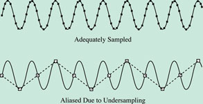
According to the Nyquist theorem, a signal must be sampled at least twice the rate of the maximum frequency component in that signal to prevent aliasing. The frequency at one-half the sampling frequency is referred to as the Nyquist frequency. Theoretically, it is possible to recover information about signals with frequencies at or below the Nyquist frequency. Frequencies above the Nyquist frequency will alias to appear between DC and the Nyquist frequency. For example, audio signals converted to electrical signals by a microphone commonly have frequency components up to 20 kHz. A board with a sampling rate greater than 40 kSps is needed to properly acquire this signal.
Sampling methods. When acquiring data from several input channels, the analog multiplexer connects each signal to the ADC at a constant rate. This method, known as continuous scanning, is significantly less expensive than having a separate amplifier and ADC for each input channel. Because the multiplexer switches between channels, a time skew is generated between each channel sample. This method is appropriate for applications where the time relationship between sampled points is unimportant. For those applications where the time relationship between inputs is important (such as phase analysis of AC signals), simultaneously sampling is necessary. DAQ products capable of simultaneous sampling use sample-and-hold circuitry for each input channel. An analog multiplexer connects one of the input signals to the ADC for processing.
It is possible to simulate simultaneous sampling hardware without paying for additional sample-and-hold circuitry. Interval scanning creates the effect of simultaneous sampling for low-frequency signals, such as temperature and pressure, while maintaining the cost benefits of continuous scanning. This method scans the input channels at one interval and uses a second interval to determine the time before repeating the scan. The input channels are scanned within microseconds, creating the effect of simultaneously sampling the input channels.
Multiplexing. A common technique for measuring several signals with a single ADC is multiplexing. A multiplexer selects and routes one channel to the ADC for digitising, then switches to another channel and repeats. Because the same ADC is sampling many channels, the effective rate of each individual channel is reduced in proportion to the number of channels sampled. As an example, a PCI-MIO-16E-1 sampling at 1,25 MSps on 10 channels will effectively sample each individual channel at 125 kSps per channel.
External analog multiplexers can often be used to increase the number of channels a board can measure. For example, SCXI uses multiplexing modules to expand the number of input channels up to 3072 with a single board. With the AMUX-64T analog multiplexer, up to 256 signals can be measured with a single board. The sampling rate is reduced proportionately by this additional external multiplexing.
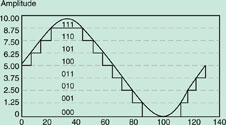
Resolution. The number of bits that the ADC uses to represent the analog signal is the resolution. The higher the resolution, the higher the number of divisions the voltage range is broken into, and therefore, the smaller the detectable voltage change. Figure 3 shows a sine wave and its corresponding digital image as obtained by an ideal 3-bit ADC. A 3-bit converter divides the analog range into 23 or eight divisions. Each division is represented by a binary code between 000 and 111. Clearly, the digital representation is not a good representation of the original analog signal because information has been lost in the conversion. By increasing the resolution to 16 bits, however, the number of codes from the ADC increases from eight to 65 536 and an extremely accurate digital representation can therefore be obtained of the analog signal if the rest of the analog input circuitry is designed properly.
Range. Range refers to the minimum and maximum voltage levels that the ADC can span. The multifunction DAQ boards offer selectable ranges so that the board is configurable to handle a variety of different voltage levels. With this flexibility, you can match the signal range to that of the ADC to take best advantage of the resolution available to accurately measure the signal.
The range, resolution and gain available on a DAQ board determine the smallest detectable change in voltage. This change in voltage represents 1 LSB of the digital value, and is often called the code width. The ideal code width is found by dividing the voltage range by the gain times two raised to the order of bits in the resolution. For example, one of National Instruments’ 16-bit multifunction DAQ boards, the AT-MIO-16XE-10, has a selectable range of 0 to 10 or -10 to 10 V and selectable gain of 1, 2, 5, 10, 20, 50 or 100. With a voltage range of 0 to 10 V, and a gain of 100, the ideal code width is:
Therefore, the theoretical resolution of one bit in the digitised value is 1,5 μV.
Critical considerations of analog inputs. Although the basic specifications previously described may show that a DAQ board has a 16-bit resolution ADC with a 100 kSps sampling rate, this does not mean that all 16 channels can be sampled at 100 kSs while retaining 16-bit accuracy. For example, products can be purchased on the market today with 16-bit ADCs that get less than 12 bits of useful data. Specifications must be scrutinised to determine if the board will give the desired results. While evaluating DAQ products, the DNL, relative accuracy, settling time of the instrumentation amplifier and noise specifications should be considered.
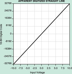
Differential nonlinearity (DNL). Ideally, as the level of voltage applied to a DAQ board increases, the digital codes from the ADC should also increase linearly. If the voltage versus the output code were plotted from an ideal ADC, the plot would be a straight line (see Figure 4a). Deviations from this ideal straight line are specified as nonlinearity.
The ideal analog code width defines the analog unit called the least significant bit (LSB). DNL is a measure in LSB of the worst-case deviation of code widths from their ideal value of 1 LSB. A perfect DAQ board has a DNL of 0 LSB. Practically, a good DAQ board will have a DNL within ±0,5 LSB.
There is no upper limit on how wide a code can be. Codes do not have widths less than 0 LSB, so the DNL is never worse than -1 LSB. A DAQ board with poor performance may have a code width equal to or very near zero, which indicates a missing code. No matter what voltage is input to the DAQ board with a missing code, the board will never digitise the voltage to the value represented by this code. Sometimes DNL is specified by stating that a DAQ board has no missing codes. This statement means only that the DNL is bounded below by -1 LSB but says nothing about its upper boundary. All National Instruments’ boards are guaranteed to have no missing codes, and the specifications clearly state the DNL of the board.
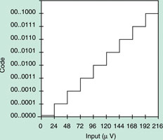
DNL can be thought of in terms of walking up a staircase. For a board with perfect DNL, each step is a perfect height and width. But for boards with poor DNL, or missing codes, the steps are not uniform; some are longer, others are taller than the ideal step (see Figure 5). If the DAQ board in the previous example, which had a code width of 1,5 μV, had a missing code slightly above 500 μV, then increasing the voltage to 502 μV would not be detectable. Only when the voltage is increased another LSB, or beyond 503 µV, will the voltage change be detectable. Poor DNL reduces the accuracy of the board.
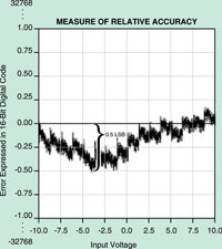
Relative accuracy. Relative accuracy is the measure in LSBs of the worst-case deviation from the ideal DAQ board transfer function of a straight line. Relative accuracy of a DAQ board can be determined by sweeping an applied voltage from the negative to positive full scale voltage and digitising it. Plotting the digitised points results in an apparent straight line (see Figure 4a). If, however, an actual straight-line (calculated) is subtracted from the digitised values and the resulting points are plotted, as shown in Figure 4b, a deviation from zero is seen. The maximum deviation from zero is the relative accuracy of the DAQ board.
Good relative accuracy is important for a DAQ board because it ensures that the translation from the actual voltage value to the binary code of the ADC is accurate. Obtaining good relative accuracy requires proper design of both the ADC and the surrounding analog circuitry.
Settling time. On a typical plug-in DAQ board, an analog signal is first selected by a multiplexer, and then amplified by an instrumentation amplifier before it is converted to a digital signal by the ADC. This instrumentation amplifier must be able to track the output of the multiplexer as it switches channels, and also to settle quickly to the accuracy of the ADC (Figure 6). Otherwise, the ADC will convert an analog signal that is still in transition from the previous channel value to the current channel value being measured. The duration required for the instrumentation amplifier to settle to a specified accuracy is called the settling time. Poor settling time is a major problem because the amount of inaccuracy usually varies with gain and sampling rate. Because these errors occur in the analog stages of the DAQ board, the board cannot return an error message to the computer when the instrumentation amplifier does not settle.
The instrumentation amplifier is most likely not to settle when it is sampling several channels at high gains and high rates. Under such conditions, the instrumentation amplifier has difficulty tracking large voltage differences that can occur as the multiplexer switches between input signals. The higher the gain and the shorter the channel switching time, the less likely it is that the instrumentation amplifier will settle. In fact, according to National Instruments, at the time of writing this article, no off-the-shelf programmable-gain instrumentation amplifier can settle to 12-bit accuracy in less than 2 μs when amplifying at a gain of 100. That is why the company developed the NI-PGIA specifically for DAQ board applications – so that boards using the NI-PGIA can settle at high gains and sampling rates.
Noise. Values that appear in the digitised signal that are different from the actual signal are called noise. Because the PC is a noisy digital environment, acquiring data on a plug-in board requires very careful layout on multilayer DAQ boards by skilled analog designers. Simply placing an ADC, instrumentation amplifier, and bus interface circuitry on a one- or two-layer board will most likely result in a very noisy DAQ board. Designers can use metal shielding on a DAQ board to help reduce noise. Proper shielding should not only be added around sensitive analog sections on a DAQ board, but must also be built into the layers of the DAQ board with ground planes.
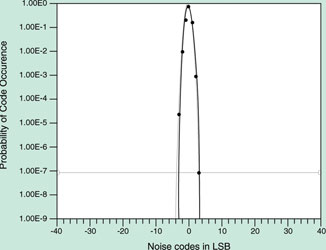
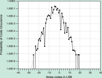
Figure 7 shows the DC noise plot of two DAQ products, both of which use the same ADC. Two qualities of the DAQ board can be determined from the noise plots – range of noise and the distribution. The plot in Figure 7a has a high distribution of samples at 0 and a very small number of points occurring at other codes. The distribution is Gaussian, which is what is expected from random noise. From the plot, the peak noise level is within ±3 LSB. The plot in Figure 7b is a very noisy DAQ product that has a much different distribution. It has noise greater than 20 LSB, with many samples occurring at points other than the expected value. For the DAQ products in Figure 7, the test was run with an input range of ±10 V and a gain of 10. Therefore, 1 LSB = 31 μV, so a noise level of 20 LSB is equivalent to 620 μV of noise.
Analog outputs. Analog output circuitry is often required to provide stimuli for a DAQ system. Several specifications for DACs determine the quality of the output signal produced – settling time, slew rate and resolution. Settling time and slew rate work together in determining how fast the DAC can change the level of the output signal. Settling time is the time required for the output to reach the specified accuracy. The settling time is usually specified for a full-scale change in voltage. The slew rate is the maximum rate of change that the DAC can produce on the output signal. Therefore, a DAC with a low settling time and a high slew rate can generate high-frequency signals, because little time is needed to accurately change the output to a new voltage level.
An example of an application that requires high performance in these parameters is the generation of audio signals. The DAC requires a high slew rate and small settling time to generate the high frequencies necessary to cover the audio range. In contrast, an example of an application that does not require fast D/A conversion is a voltage source that controls a heater. Because the heater cannot respond quickly to a voltage change, fast D/A conversion is not necessary. The application will determine the DAC specifications.
Output resolution is similar to input resolution. It is the number of bits in the digital code that generates the analog output. A larger number of bits reduces the magnitude of each output voltage increment, thereby making it possible to generate smoothly changing signals. Applications requiring a wide dynamic range with small incremental voltage changes in the analog output signal may need high-resolution voltage outputs.
Digital I/O – DIO interfaces are often used on PC DAQ systems to control processes, generate patterns for testing, and communicate with peripheral equipment. In each case, the important parameters include the number of digital lines available, the rate at which digital data can be accepted and sourced, and the drive capability of the lines.
If the digital lines are used for controlling events such as turning on and off heaters, motors or lights, a high data rate is usually not required because the equipment cannot respond very quickly. The number of digital lines, of course, needs to match the number of items that are controlled. In each of these examples, the amount of current required to turn the devices on and off must be less than the available drive current from the board.
With the proper digital signal conditioning accessories, however, the low current TTL signals of the DAQ hardware can be used to monitor and control high voltage and current signals from industrial hardware. For example, the voltage and current needed to open and close a large valve may be on the order of 100 V a.c. at 2 A. Because the output of a digital I/O board is 0 to 5 V d.c. at several milliamperes, an SSR series, ER-8/16, SC-206X series or SCXI module is needed to switch the power signal to control the valve.
A common application is to transfer data between a computer and equipment such as data loggers, data processors and printers. Because this equipment usually transfers data in 1-Byte (8-bit) increments, the digital lines on a plug-in digital I/O board are arranged in groups of eight. In addition, some boards with digital capabilities will have handshaking circuitry for communication synchronisation purposes. The number of channels, data rate and handshaking capabilities are all important specifications that should be understood and matched to the application.
This article will be continued in a future edition of Dataweek.
For more information contact National Instruments, 0800 203 199.


© Technews Publishing (Pty) Ltd | All Rights Reserved
 printer friendly version