


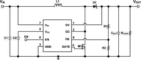
Exar is preparing to introduce a family of new boost controllers that have internal compensation, enabling a reduction in external component count in certain applications.
But there are limitations; boost and buck-boost converters operating in continuous conduction mode (CCM) have a right-half-plane (RHP) zero associated with their system transfer function.
RHP zero is the tendency of the converter to initially respond to a circuit disturbance in the opposite direction to that commanded by the controlling signal, otherwise known as positive feedback. For example, if there is a sudden increase in the load drawn from a boost converter, its output voltage will droop and the converter will respond with a longer duty cycle. However, a longer switch on time will result in a shorter diode conduction time which charges the output capacitor and will initially cause further droop in output voltage.
This is confusing to the controller and the only solution is to wait and see what the long term trend is before adjusting the duty cycle. In order to achieve this, the crossover frequency, fC, should be lower than the RHP zero frequency. Another solution to deal with RHP zero is to design the converter to operate in discontinuous conduction mode (DCM) over the full range of operating conditions. Each of the two methods will be discussed below.
Removing the effect of RHP zero by operating in DCM
The control-to-output transfer function of a boost or buck-boost converter operating in DCM has a single pole. In DCM the inductor energy is completely discharged during every switching cycle (ie, inductor current is reduced to zero). The transfer function of boost and buck-boost converters changes in DCM. The small inductor value used to ensure DCM (small relative to the inductor value in CCM operation) causes the RHP zero frequency to be shifted close to the switching frequency. Hence the RHP zero is of no consequence when compensating the feedback loop. Additionally, the frequency of the pole associated with the inductor is also moved to a high frequency.
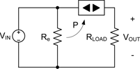
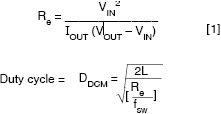
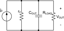
To understand the DCM operation in detail, first we need to transform the DCM boost converter into a loss-free resistor model. The DC equivalent circuit for a DCM boost converter is shown in Figure 2. The MOSFET behaves as an effective resistor, Re, and the diode behaves as a power source. The loss-free resistor model states that the power consumed by the effective resistor should be equal to the power consumed by the power source[1].
Therefore,
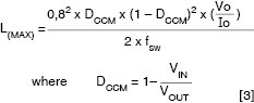
Where fsw = 600 kHz for the new device. [2]
The maximum inductance to keep the boost converter running in DCM is
Now we need to transform the DCM boost converter into an AC equivalent circuit. The DCM boost converter small signal model at the output is shown in Figure 3 where
and
Therefore the DC gain will be
and the pole will be
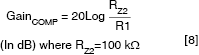
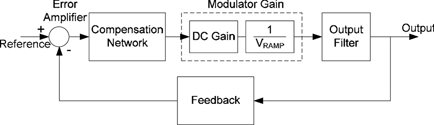
Since there is one pole in the system, a simple single-pole single-zero compensating network (type II compensation) can be used to stabilise the system as in Figure 4. The new device has a built-in type II compensation network which reduces the use of external components.
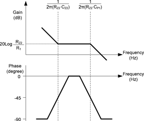
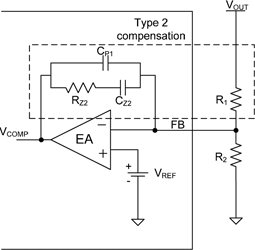
The new device’s internal compensated pole and zero are located at 6,4 kHz and 796 kHz respectively. Thus, the compensation gain is equal to:
The new device has an input voltage feed forward compensation, which helps to maintain the same DC gain over its input voltage range.
The system’s overall control loop is shown in Figure 6.
Example 1. VIN = 12 V, VOUT = 30 V, IOUT = 400 mA
1. Find the maximum inductance we can use by equation (3).
Higher inductance will reduce the inductor peak current and thus increase the efficiency. Therefore, a standard 3,3 μH inductor is chosen for this application.
2. Calculate the correct output capacitance to set the pole location by using equations (1), (5) and (7). The pole frequency should be located between 500 Hz and 6 kHz to maintain at least a 45° phase margin. Using a larger capacitance helps to reduce the output ripple. In this case, we choose to locate the pole at 500 Hz. A standard 10 μF capacitor is chosen to set the pole at fP = 560 Hz.
3. Choose R1 to set the crossover frequency. The crossover frequency should be less than one tenth of its switching frequency, which will be 60 kHz for the new device. We choose fC = 20 kHz in this case.
We pick a standard 100 kΩ resistor for R1 to set the crossover frequency at 24 kHz, and the phase margin is 75°.
Challenges of CCM voltage-mode boost converter loop compensation
As discussed, a boost converter operating in CCM has a RHP zero that complicates the loop compensation. The RHP zero limits the converter bandwidth (ie, limits crossover frequency fC) and may require increasing the output filter capacitor in order for loop compensation to be possible.
This makes loop compensation of a CCM boost converter challenging for controllers that have internal compensation, such as the new device. Another option is to use the SP6136, a voltage mode buck controller with external compensation which overcomes the compensation challenges. CCM operation has the advantage of lower peak switch and inductor current compared to a converter operating in DCM. This will result in reduced power dissipation and possibly reduced size of the switch, diode, input capacitor and output capacitor.
The inductor size is actually minimised in the DCM case because 100% of the energy is transferred to the output each cycle.
The control-to-output gain of a CCM boost converter is shown in Figure 8. Here the important features are specified in terms of input inductor L, output capacitor COUT, duty cycle D and load resistance RLOAD. It is assumed that the low ESR of COUT results in fESR being higher than fRHP. Note that fRHP is load dependent and should be evaluated for the highest load current (ie, lowest RLOAD). In order to safeguard against the RHP zero’s destabilising effect, the crossover frequency fC should be placed at less than one third of fRHP[2]. This places an upper limit on fC and limits converter bandwidth.
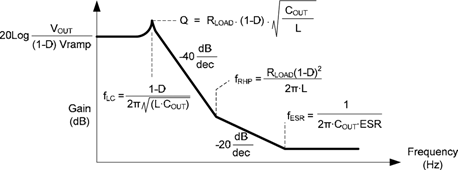
Also note that there is the usual load dependent peaking associated with the double pole at fLC. To reduce the effect of peaking on the crossover frequency, we will place fC at a frequency at least three times higher than fLC. Since fC should be less than one third of fRHP, then fLC must be less than one ninth of fRHP. Thus the two requirements for compensating the loop are:
FLC = 0,1 x fRHP
FC = 0,33 x fRHP
In order to satisfy the first requirement, L and COUT should be selected using the usual design guidelines for a CCM boost converter. If necessary, COUT must be increased such that fLC ≤ 0,1 x fRHP. Once L and COUT are selected, the features of the gain plot shown in Figure 8 are explicitly defined.
Now a type-III compensator must be tailored such that fC is forced to cross over at the required frequency of 0,33 x fRHP.
The following example will help to better illustrate the steps required for the loop compensation of a CCM boost converter.
Example: Design a non-synchronous boost converter to meet the following requirements: VIN = 12 V, VOUT = 30 V, IOUT(max) = 400 mA, IOUT(min) = 100 mA, fSW = 600 kHz, VRAMP = 1 V, VRIPPLE = 1%. The converter must operate in CCM over the specified IOUT range.
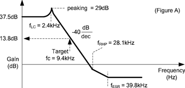
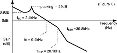
Solution: Following conventional design procedures, L and COUT are calculated to be 60 μH and 1 μF respectively. Select standard values of 68 μH and 1 μF. Duty cycle is approximately 0,6. From the equations shown in Figure 8, fLC = 7,7 kHz and fRHP = 28,1 kHz.
By increasing COUT to 10 μF, fLC is reduced to 2,4 kHz and the first requirement is satisfied. Assuming ESR = 0,4 Ω then fESR = 39,8 kHz, and fC should be placed at 9,4 kHz in order to satisfy the second requirement. The gain at 9,4 kHz is 13,8 dB as shown in Figure 9a. Therefore the compensation network must have a gain of -13,8 dB at 9,4 kHz (Figure 9b). As can be seen from the high Q, the phase change at fLC will be abrupt. To counter the sudden decrease in phase, the zeros must be placed at 70% of fLC. Therefore the two zeros should be placed at 1,7 kHz (Figure 9b).
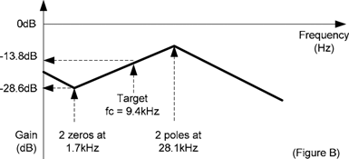
The zero’s corresponding gain will be:
-13,8 dB - [20 dB (log(1,7 kHz/9,4 kHz))] = -28,6 dB (Figure 9b).
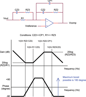
Refer to Figure 10 which shows the type-III compensation and solve the equations:
Let R1 = 200 kΩ
20Log(RZ2/R1) = -28,6 dB therefore RZ2 = 7,43 kΩ
1/(2π RZ2CZ2) = 1,7 kHz therefore CZ2 = 13000 pF
1/(2π R1CZ3) = 1,7 kHz therefore CZ3 = 468 pF
Place the two poles at fRHP:
1/(2π RZ2CP1) = 28,1 kHz therefore CP1 = 763 pF
1/(2π RZ3CZ3) = 28,1 kHz therefore RZ3 = 12,1 kΩ
A type-III compensator with the above components will result in a compensator gain shown in Figure 9b and overall converter gain shown in Figure 9c. The converter should have a phase margin of 50–70° at fC.
Note that the phase lead of RHP zero will cancel the phase lag of ESR since fRHP is close to fESR. Also, the phase lead of two zeros at 1,7 kHz should almost cancel the phase lag of fLC at 2,4 kHz. Then the net phase at fC is somewhat lower than -90° which corresponds to the desired phase margin of 50–70°.
In the example above, zeros are required at 1,7 kHz, versus the internal value of 6,4 kHz for the new device. As a result, it became necessary to use the SP6136 buck controller configured in a boost configuration. The SP6136 operates at the same 600 kHz as the device, but has external compensation available to the designer, so that the control loop can be optimised to deal with the RHP zero without radically modifying the power train components.
Conclusions
When designing a boost circuit with voltage mode control, extra caution must be taken to ensure that the circuit is stable.
Exar’s new device has internal compensation to reduce component count, but this reduces compensation flexibility. In the example above, VIN = 12 V, VOUT = 30 V at 400 mA, the device was best designed in DCM mode. For CCM operation, the same set of input and output conditions required compensation values beyond what the new device could support. Thus the SP6136 controller was chosen to allow for external compensation.
Although the device was unable to provide a CCM solution in this case, both the LC double pole and the RHP zero are functions of the duty cycle and for output voltages closer to the input voltage, the device can provide both DCM and CCM solutions.
Lastly, a note regarding designs relying on DCM operation: make sure they stay in DCM operation. If a circuit designed for DCM operation begins operating in CCM mode, it is likely to become unstable. However, a CCM design will almost always be stable in DCM mode.
References
[1] Robert W. Erickson and Dragan Maksimovic, Fundamentals of Power Electronics, 2nd edition, 2005.
[2] Ray Ridley, Switching Power, 2006 to the desired phase margin of 50–70°.
| Tel: | +27 11 854 5011 |
| Email: | sales@khd.co.za |
| www: | www.khd.co.za |
| Articles: | More information and articles about KH Distributors |


© Technews Publishing (Pty) Ltd | All Rights Reserved
 printer friendly version