


Anyone involved in high-speed data capture designs that use an FPGA has probably heard the buzzword for the new JEDEC standard: JESD204B. Recently a lot of engineers have contacted Texas Instruments requesting information on the JESD204B interface, including how it works with an FPGA and how it will make their designs easier to execute.
This article discusses the evolution of the JESD204B standard and what it means to a systems design engineer.
What led to the JESD204B standard?
About 10 years ago, designers of high-speed data converters switched from using the traditional single-ended CMOS interface to using a differential LVDS interface because the latter enabled higher data rates (the CMOS interface is limited to about 200 Mbps.)
The LVDS interface also improved noise coupling on signal lines and power supplies. The drawback of this interface was higher power consumption at lower sampling speeds. This gave the CMOS interface a reason for existence, and it is still being used today.
With the evolution of analog-to-digital converters (ADCs) requiring faster sampling rates and higher channel density, the industry was demanding a faster, more power-efficient digital interface than parallel LVDS. In order to overcome this challenge, a true serial interface called JESD204 was developed and approved by JEDEC in April 2006.
The JESD204 interface is defined as a single-lane, high-speed serial link connecting single or multiple data converters to a digital logic device with data rates of up to 3,125 Gbps. It needs a common frame clock sent to the converter and the FPGA to synchronise the frames.
Supporting only one lane and one serial link, JESD204 was soon viewed as not quite as useful as initially hoped, so in April 2008 the standard was revised to JESD204A. This extended support for multiple aligned lanes and multipoint links, but the maximum speed was still limited to 3,125 Gbps.
This drove the development in July 2011 of JESD204B, which promises to address several different system design challenges. Besides drastically increasing the supported data rates from 3,125 Gbps to 12,5 Gbps, it also greatly simplifies multichannel synchronisation by adding the deterministic latency feature.
What is the JESD204B standard?
JESD204B supports interface speeds of up to 12,5 Gbps, uses a device clock instead of the previously used frame clock, and has three different subclasses. Subclass 0 is backward compatible with JESD204A except at higher speeds, and it does not support deterministic latency.
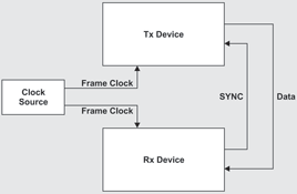
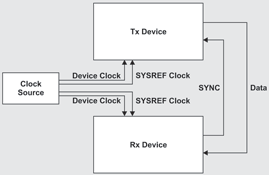
Furthermore, the SYNC signal has special timing requirements for error reporting (Figure 1). Subclass 1 uses synchronisation signal SYSREF to initiate and align the local multi-frame clocks across devices (Figure 2). This synchronises data transmission and achieves a known, deterministic latency across the digital link.
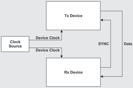
Subclass 2 uses the SYNC signal for that same purpose (Figure 3). Due to SYNC timing constraints, Subclass 2 is typically employed for data rates lower than 500 MSps. For speeds higher than this, Subclass 1 with an external SYSREF clock is commonly preferred.
JESD204B-compliant receivers are outfitted with an elastic buffer that is used to compensate for skew across serialiser/deserialiser (SerDes) lanes, which simplifies board layout. This elastic buffer stores the data until the data from the slowest lane arrives, at which time it releases the data from all lanes simultaneously for digital processing.
This skew management is possible because the data clock is embedded in the serial data stream.
Why care about the JESD204B interface?
Since JESD204B-compliant data converters serialise and transmit output data at a much higher rate than with previous interfaces, the number of pins required on the data converters as well as on processors or FPGAs is drastically reduced, translating to smaller package sizes and lower cost. However, the biggest benefits from the reduced pin count may be a much simpler layout on the printed circuit board (PCB) and easier routing because there are much fewer lanes on the board.
Layout and routing are further simplified by the reduced need for skew management, which is made possible by the data clock now being embedded in the data stream and the presence of the elastic buffer in the receiver. Hence, the need for trace squiggles to match lengths is eliminated.
The JESD204B standard also allows longer transmission distances. Relaxed skew requirements enable logic devices to be placed much farther from data converters to avoid any impact on sensitive analog parts. Additionally, the JESD204B interface is adaptable to different resolutions of data converters. This removes the need for physical redesign of transceiver/receiver (Tx/Rx) boards (logic devices) for future ADCs and digital-to-analog converters (DACs).
Does this mean the end for the LVDS interface?
The CMOS interface provides lower power consumption for data converters with lower data rates, while the JESD204B interface offers a few benefits over the traditional LVDS interface. So does the LVDS interface have any chance of survival?
The simple answer is yes. While the JESD204B standard has simplified multichannel synchronisation by using deterministic latency, there are applications that require minimal latency (and, in an ideal world, no latency). These applications (for example, aerospace applications like radar) need an immediate response to an action or detection; any possible delay must be minimised. For these applications, the LVDS interface should be considered, since the JESD204B-compliant data converter’s delay in serialising the data is omitted.
For more information contact Erich Nast, Avnet Kopp, +27 (0)11 319 8600, [email protected], www.avnet.co.za


© Technews Publishing (Pty) Ltd | All Rights Reserved
 printer friendly version