


Mobile network operators are increasingly turning to small cell base stations to expand coverage, increase capacity and enable network densification in congested, high-traffic urban environments. Small cells are low-power radio access nodes that can be used by operators to offload mobile data to Internet Protocol (IP) networks and enable more efficient use of radio spectrum in 4G/LTE applications. Small cells are playing a critical role in helping service providers address escalating bandwidth demand.
To fully realise the benefits small cells will provide, they must first be optimised in terms of size, power, performance and cost. This is critical because small cells must be deployed in compact, space-constrained, non-temperature-controlled outdoor locations. Minimal power consumption is important because small cells are often powered using Power over Ethernet (PoE) solutions.
To date, significant effort has been made to optimise baseband system-on-chip (SoC) and digital radio front end performance and integration. This article focuses on a portion of the small cell design that is often overlooked: timing and clock synthesis. New IC architectures are now available that enable lower power, smaller form factor and higher-performance small cell clock synthesis.
Architectures for low phase noise integer-N PLLs
There are two approaches to building chip architectures for low phase noise integer-N PLLs (phase-locked loops) used in small cell applications. Figure 1 shows the conventional analog architecture used to implement a jitter attenuating PLL for wireless infrastructure applications.
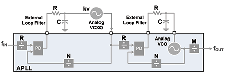
This two-stage cascaded PLL architecture uses a discrete, analog narrowband VCXO-based PLL to implement jitter cleaning in the first loop. The VCXO is used as the PLL VCO because of its low phase noise. The second stage PLL relies on an analog wideband PLL to provide clock multiplication. The conventional architecture requires discrete loop filter components in addition to the discrete VCXO.
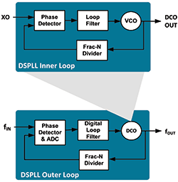
Figure 2 shows an alternative approach using Silicon Labs’ proprietary fourth-generation DSPLL architecture. DSPLL technology uses a dual-loop PLL architecture with an inner loop and outer loop to realise a low-bandwidth, jitter attenuating PLL. The inner loop works as a digitally controlled oscillator (DCO) for the outer loop. The inner loop is a wideband PLL based on a low phase noise 15 GHz analog LC oscillator.
Rather than controlling the VCO using analog circuitry, the oscillator is digitally steered using a high-resolution fractional-N feedback divider. The fractional-N feedback divider is modulated in precise steps to enable the entire inner loop to operate as a DCO.
The LC oscillator provides a wide tuning range, enabling the inner loop PLL to operate over a wide frequency range. A low-cost fundamental mode, non-pullable crystal is used as the inner loop reference, and the loop filter function is implemented digitally without the need for discrete components.
The DSPLL outer loop performs three functions: synchronisation to an externally provided reference clock, jitter attenuation and clock multiplication. Since the inner loop is digitally controlled, the DSPLL outer loop can similarly be implemented using a highly digital architecture. The DSPLL outer loop filter is entirely implemented on-chip using an advanced analog-to-digital converter (ADC) and digital signal processing (DSP) based architecture, simplifying printed-circuit board (PCB) layout and design and maximising immunity to board-level noise.
An added benefit of this architecture is user-programmability of critical PLL parameters such as the PLL loop bandwidth. The effective frequency tuning resolution of this architecture is 1 part per trillion (ppt), enabling very precise PLL control. Furthermore, the DSPLL architecture requires no bill of materials (BOM) changes to support different input and output frequencies and loop bandwidths.
DSPLL phase noise optimisation
Silicon Labs’ proprietary DSPLL architecture has been developed and refined over the last 15 years to provide ultra-low phase noise clock generation for high-speed data converters and 10/40/100G transceivers. Figure 3 illustrates how its fourth-generation DSPLL has been optimised for phase noise. In this example, all frequencies have been normalised to 1 GHz.
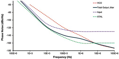
At close-in offset frequencies, the DSPLL architecture’s phase noise closely follows the crystal used as a reference for the inner loop. The architecture uses a low-cost, fundamental mode, non-pullable crystal with excellent close-in phase noise. At higher offsets (~1 MHz), DSPLL phase noise follows the voltage-controlled oscillator (VCO).
Silicon Labs’ technology uses an ultra-low phase noise LC oscillator designed in the most advanced CMOS process node used in the timing industry (55 nm) to achieve very low phase noise at high offset frequencies. The phase noise at the DSPLL output (shown in dark blue in Figure 3) is a combination of these elements, providing optimal performance in a fully integrated solution.
The loop bandwidth of the DSPLL can be digitally programmed by the developer to set the point at which the reference clock jitter is filtered (~1 kHz in this example). If the input has relatively low phase noise at close-in offset frequencies, a higher DSPLL loop bandwidth is recommended. If the clock input has higher close-in phase noise, a lower DSPLL loop bandwidth is preferred.
The programmability of the DSPLL loop bandwidth enables customers to optimise jitter transfer versus jitter generation to achieve the lowest phase noise possible depending on input conditions.
Advantages of the DSPLL architecture
The single-oscillator DSPLL architecture provides unparalleled integration and flexibility compared to conventional, two-oscillator analog cascaded PLL architectures. While these two architectures provide similar functions, including jitter attenuation and clock multiplication, there are significant differences in terms of PCB footprint, power consumption and performance.
PCB footprint
Table 1 compares the PCB footprint of the two architectures. Note that this comparison is a sum of component area only, without regard to PCB spacing or design rules.
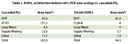
The DSPLL PCB footprint is three times smaller than the cascaded PLL due to a combination of factors. The DSPLL does not require a large, bulky VCXO, simplifying the PCB layout and design while minimising the total solution cost. The DSPLL loop filters are integrated on chip, further simplifying the PCB layout. The DSPLL uses multiple on-chip voltage regulators to filter board-level supply noise and minimise the need for discrete filtering components.
In contrast, cascaded PLLs require more dedicated power supplies, each with its own unique filtering requirements. DSPLL-based products do not require a low dropout (LDO) regulator, while the cascaded PLL’s VCO is sensitive to noise injection and requires an external LDO for power supply filtering.
The DSPLL architecture’s small footprint makes it a better choice for space-constrained small cell, pico cell and mobile backhaul applications.
Power consumption
There is a significant difference in power consumption between cascaded PLL and DSPLL-based clock devices. Table 2 shows the typical power consumption of the two options. The unique, all-digital DSPLL architecture is more power efficient, consuming more than 30% less power than analog PLL-based cascaded PLL devices.
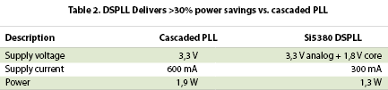
Silicon Labs’ fourth-generation DSPLL-based products combine advanced process technology with an efficient, digital-intensive architecture to deliver significant power savings versus conventional solutions. A power efficient architecture is especially important for PoE-powered small cells and pico cells given their limited power budget.
Phase noise performance
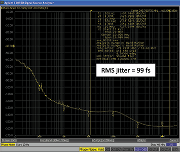
Cascaded PLLs rely on discrete voltage-controlled crystal oscillators (VCXOs) to deliver excellent phase noise and jitter performance (see Figure 4). On the other hand, these solutions are more susceptible to board-level noise since each of the discrete nodes in the architecture, including the charge pump output, loop filter and VCXO, is a potential point for noise entry.
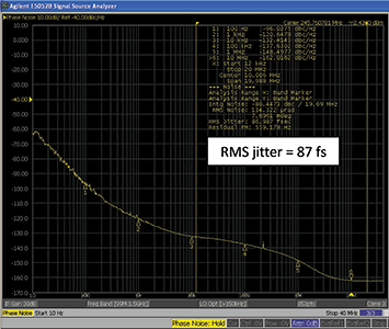
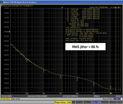
The DSPLL architecture delivers even better phase noise performance as cascaded PLL + VCXO arrangements without the need for discrete VCXOs, loop filters or LDOs (see Figure 5). As an added benefit, DSPLL-based products are more immune to board-level noise since the architecture is fully integrated.
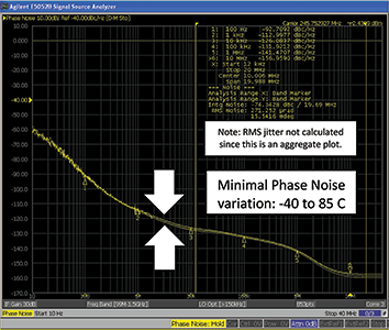
An added benefit of the DSPLL architecture is highly consistent performance over temperature. Figure 6 shows the DSPLL architecture’s phase noise at -40°C, 0°C and 85°C. Consistent phase noise performance is critical in small cell and repeater applications since this equipment is typically deployed in a non-temperature-controlled environment. The measurement below assumes a highly jittered reference clock is provided as an input to the DSPLL.
Loop filter integration and adjustable jitter attenuation
Cascaded PLLs require external loop filters for PLL1 and PLL2. Given that these components are off-chip, they are sensitive to board-level noise getting into the PLL and impacting device jitter and phase noise. In contrast, the DSPLL architecture’s loop filters are on-chip, providing higher immunity to board-level noise.
The PLL bandwidths of a cascaded PLL design are fixed. With their discrete architecture, the only way to change the PLL bandwidth is to change the loop filter component values. This makes it difficult to fine-tune the PLL bandwidth to optimise jitter attenuation at the application level. In contrast, the outer loop bandwidth of the DSPLL can be simply programmed via device registers without the need for external BOM changes.
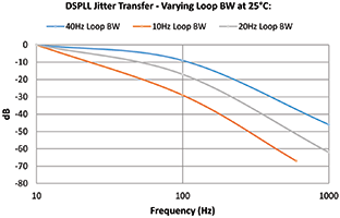
Figure 7 shows how lowering the DSPLL loop bandwidth results in greater attenuation of the reference clock jitter. The device loop bandwidth can be simply programmed via registers without the need to calculate loop filter component values or the PLL’s phase margin, simplifying design.
Jitter transfer
A narrowband PLL must be able to tolerate a significant amount of jitter on its input without losing PLL lock, filter the noise on its reference clock and minimise the amount of jitter transferred to its output. This is especially critical in applications where the narrowband PLL is synchronised to a line-recovered clock from a clock and data recovery (CDR) IC such as a common public radio interface (CPRI) or CPRI over optical transport network (OTN) device.
A PLL’s jitter transfer function is a ratio of its output jitter spectrum to the applied input jitter spectrum. A well designed, high-performance PLL will demonstrate low jitter peaking at the PLL bandwidth and consistent operation over temperature.
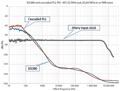
As shown in Figure 8, DSPLL delivers comparable jitter transfer performance in comparison to conventional cascaded PLLs when synchronised to a high jitter input clock. However, DSPLL provides superior loop bandwidth flexibility since it is digitally programmable by the user, enabling them to optimise jitter performance even after the PCB is fabricated.
In addition, the DSPLL architecture delivers highly consistent performance over temperature (see Figure 6), ensuring repeatable performance across operating conditions. Excellent jitter transfer performance helps to simplify HetNet network deployments since it enables small cells and pico cells to be installed farther away from supporting infrastructure.
Short-term holdover
High-performance PLLs need to provide a stable, accurate output clock even if there is a problem with the upstream PLL driving the timing synchronisation chain. If the upstream PLL’s clock goes away, the downstream PLL needs to enter holdover and provide an accurate output clock until the upstream PLL’s clock reappears. During this holdover period, the accuracy of a cascaded PLL’s output clock is largely a function of how tightly the VCXO can be held.
Cascaded PLLs typically use an on-chip digital-to-analog converter (DAC) to drive the VCXO with its last known control voltage setting. It can be difficult to hold a VCXO using this approach since this implementation is analog in nature, suffers from higher initial frequency offset error, and is susceptible to leakage and frequency drift over time.
In contrast, the DSPLL architecture uses an averaged input clock frequency as its holdover frequency to minimise the disturbance of the output clock frequency when an input clock suddenly fails. The final averaged holdover frequency value is calculated from a programmable window within the stored historical frequency data. Both the window size and the delay are programmable. This feature enables the holdover circuit to ignore frequency data that may be corrupt just before the input clock failure.
As an additional benefit, when the DSPLL exits holdover and reacquires lock to a new input clock, the pull-in process is glitch-less and controlled by the DSPLL’s outer loop bandwidth, ensuring that an abrupt frequency shift doesn’t occur.
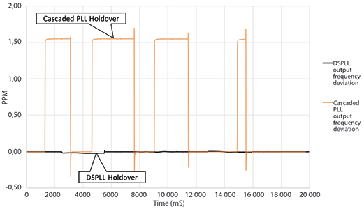
Figure 9 shows the holdover performance of the DSPLL in comparison to cascaded PLLs. The DSPLL has excellent initial frequency offset performance and, when combined with holdover averaging, provides highly stable performance in holdover applications.
Vibration effects
Because they use discrete VCXOs, cascaded PLLs are more susceptible to vibration effects. Lightly tapping the evaluation board of a cascaded PLL shows a large increase in low-frequency spurs and an elevated noise floor, as shown in Figure 10. A similar test on a timing device with DSPLL technology does not produce any spurious signals or an elevated noise floor.
Summary
Silicon Labs’ proprietary fourth-generation DSPLL architecture brings together the best of analog and digital technologies. It combines an analog low phase noise LC-VCO, a digital PLL architecture and cutting-edge 55 nm CMOS technology to provide a solution that offers higher integration, smaller form factor, lower power and more robust performance compared to conventional cascaded PLL devices. These benefits greatly simplify the design of small cells, pico cells, micro cells, point-to-point radios and mobile backhaul equipment.
For more information contact NuVision Electronics, +27 (0)11 608 0144, [email protected], www.nuvisionelec.co.za
| Tel: | +27 11 608 0144 |
| Fax: | +27 11 608 4723 |
| Email: | [email protected] |
| www: | www.nuvisionelec.com |
| Articles: | More information and articles about NuVision Electronics |


© Technews Publishing (Pty) Ltd | All Rights Reserved
 printer friendly version