The core value of condition monitoring is long-term cost saving. The cost saving is achieved through reduction in maintenance costs with predictive maintenance and the elimination of unplanned production downtime with preventive maintenance. The realisation of such value relies on the condition monitoring system’s ability to accurately detect and identify fault conditions in the early stages of development.
Unlike catastrophic failure at the very late stages of development, which can often be bluntly obvious and easily detectable, fault detection in the early stages of development may only cause a very slight deviation from the asset’s normal operating behaviour. This deviation may also be transient in nature. The proper detection and classification of early fault signatures usually requires the use of high-performance sensors of varying sensing modalities as part of the overall monitoring solution. These sensors need to be properly interfaced with DAQ signal chains of matching performance to fully utilise their sensing capability. The data can then be combined and processed using specialised algorithms to determine the overall condition of the asset being monitored.
Like all system designs, there are many choices to be made when it comes to designing a condition monitoring system. Each of these choices comes with various trade-offs and can drastically alter the DAQ signal chain design.
System-level considerations
System architecture
The first level to consider for a condition monitoring (CM) system is the system architecture. There are several common CM system architecture options based on the relative location between the sensor and the DAQ signal chain, each with certain advantages.
DAQ centralised
A typical DAQ centralised system bundles multiple data acquisition channels together in a centralised location, typically in the form of a box/rack instrument. Sensors are remotely located and connect to the DAQ system using analog cables.
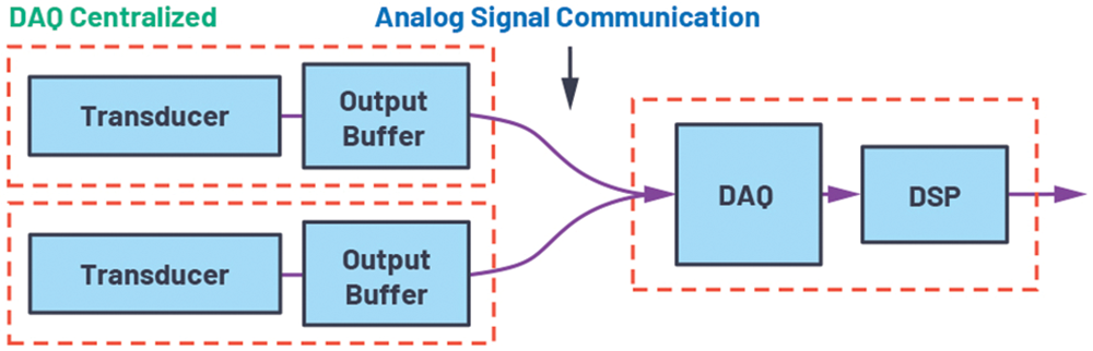 Figure 1. DAQ centralised system architecture.
The DAQ centralised architecture is widely used by many existing measurement solutions. Most benchtop vibration monitoring instruments as well as industrial analog input modules employ this architecture. It is also very suitable for designing assets with built-in CM functionality, for example, when integrating CM capability in motors and pumps.
Some of the key advantages of this architecture include:
• Low cabling cost. Low-cost coaxial and twisted pair cables are often used for carrying signals between the sensor and the DAQ over a long distance.
• Robust interface. There are a number of standard interfacing protocols, such as IEPE and the
• Flexible sensor support. The same DAQ system can be designed to support multiple sensor types based on the measurement requirements.
• Support for harsh operating environments. The physical separation of the sensor and the DAQ signal chain allows certain sensors to operate in conditions that are usually not supported by the electronic components, such as having extremely high/low operating temperature.
• More efficient DAQ signal chain implementation. The signal chain design can share more common blocks to improve efficiency and reduce cost.
The typical data acquisition signal chain design requirements for a CM system with DAQ centralised architecture are:
• Performance. Most of the DAQ centralised systems are designed to support multiple sensor types. Some of them have the dual functionality of also being used as general-purpose DAQ instruments. These needs elevate the performance requirements of the DAQ signal chain and demand metrics such as wide dynamic range, adjustable bandwidth, AC linearity and DC precision.
• Input protection. As the input terminals of the DAQ centralised system are often exposed to external access, they are susceptible to damage from the likes of miswiring, signal over-ranging and ESD. Additional protection circuitry is often required to help protect the DAQ input.
• Aliasing rejection. The vendors of systems utilising the DAQ centralised architecture do not always control the sensor and the input signal that is to be used with the system. For this reason, these systems need to be robust against the aliasing of signals and noises that are outside the measurement band of interest. Many of these systems require the DAQ to have full rejection of all out-of-band signals.
• Power and area. Compared to the other system architectures, the DAQ centralised architecture poses fewer constraints on the power consumption and solution size of the DAQ signal chain. However, some of the newer systems are pushing for higher channel density, for which the DAQ signal chain solution size and thermal density play a more important role in design considerations.
Edge node
Compared to the DAQ centralised architecture, the edge node architecture is at the other end of the spectrum in terms of solution integration level. On edge node-based systems, the sensors, DAQ signal chain and signal processing unit are all located in close proximity. The signals are sensed, acquired and processed at the edge. The processed data is sent out to the host computer using a wired or wireless communication link.
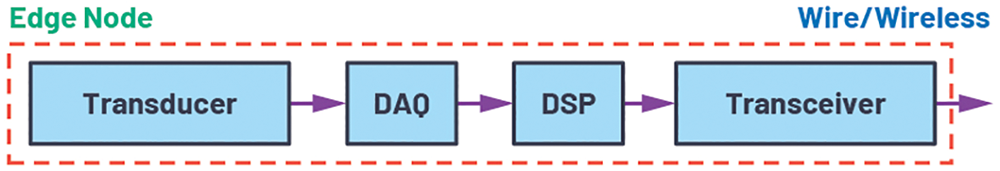 Figure 2. Edge node system architecture.
Many battery-powered smart condition monitoring systems employ edge node architecture, which has advantages such as ease of installation, especially for wireless systems, as the installation of an edge node system requires less effort in routing potentially long cables between sensing nodes. As the entire system is more defined and self-contained, it is easier to design an optimised signal chain.
The typical DAQ signal chain design requirements for a CM system with edge node architecture are:
• Performance. Knowing exactly which sensors need to be connected to the DAQ makes it possible to tailor the DAQ signal chain design and improve efficiency. However, limited power budget, especially in battery-powered systems, can limit the performance of the sensor and the signal chain.
• Input protection. Because the system is self-contained, the analog DAQ signal chain is not exposed to the outside world. This relaxes the analog DAQ signal chain input protection requirement.
• Aliasing rejection. Similarly, the short distance between the sensor and the DAQ system, together with the self-contained physical structure, make it less likely for edge node systems to pick up out-of-band interference. The DAQ system may still need some level of filtering to protect it from interference from within the node – such as from the sensor clock artifact, power supply and communication link – but the level of rejection needed is lower than that of DAQ centralised systems.
• Power and area. Low power and compact solution size are common requirements for edge node systems. Low power is essential for battery-powered systems. The size of the system impacts the system housing material cost, the ease of installation and in the case of vibration sensing systems, the mechanical characteristics of the sensor.
DAQ distributed systems
The DAQ distributed architecture sits between the DAQ centralised and edge node architectures. In this architecture, the DAQ signal chain is located at the sensor side with limited or no data processing capability. The acquired sensor data is communicated through a digital wired link such as RS-485 or 10BASE-T1L Ethernet to a centralised host for postprocessing.
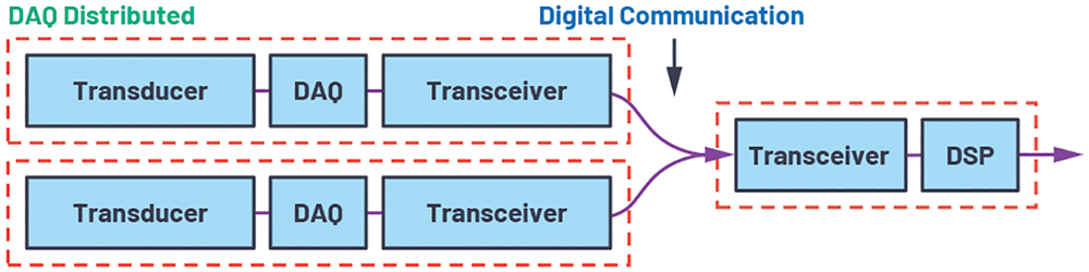 Figure 3. DAQ distributed system architecture.
The advantages of the DAQ distributed architecture include a more standardised communication interface and better integration to the bigger factory automation systems. Signal chain design considerations for the DAQ distributed system are similar to those of the edge node system.
Sensors
Sensing modality
Choosing the sensors to be used in a condition monitoring system depends on several factors, the first being the sensing modalities to support. Just like a doctor would monitor multiple vital signs of a patient for better diagnosis of his/her health condition, monitoring multiple parameters of an asset can improve the accuracy of fault detection.
For example, vibration monitoring has proven to be a reliable method for detecting mechanical failures in the early stages of development. Temperature is another important complementary parameter in CM, as many fault types can produce heat. Other common sensing modalities used in CM include sound, power quality, strain, torque and displacement. The exact combination of sensing modality required for a given CM system also depends on the asset type being monitored as well as the fault types to be detected.
Sensor type
For the same sensing modality there can also be multiple sensor types to choose from. Different types of sensors can have different properties and interfacing requirements and there is no one that suits all CM systems.
Take vibration monitoring, for example. Common vibration sensor types include MEMS, piezoelectric (piezo) and piezoresistive (dynamic strain gauge). MEMS accelerometers have low power consumption, light weight and small size, which makes them very suitable for systems with edge node architecture. Piezo accelerometers can support very wide bandwidth and have high dynamic range. Piezo sensors with the IEPE interface are compatible with many vibration monitoring instruments and can be used together to construct a CM system with the DAQ centralised architecture.
The interfacing requirements of these two types of sensors are also very different. Some MEMS accelerometers have digital output and can be hooked directly to a microprocessor. Most of the high-performance MEMS accelerometers have analog output and require a data acquisition signal chain. MEMS sensors can typically be powered by a single-ended 3,3 V to 5 V; supply shared with the DAQ signal chain. In comparison, piezo accelerometers with the IEPE interface are typically powered by a ~4 mA; constant current source generated across a 24 V; supply through a 2-wire cable, with the sensor output being an AC signal on top of a DC bias voltage (typically 8 V; to 10 V), which typically needs to be buffered, attenuated and level shifted before it can be acquired by an ADC.
Channel count
Another sensor-related consideration is the number of sensors to be used, which can directly impact the number of DAQ channels required. A CM system may deploy the same sensor type in multiple locations to provide a more complete picture of the asset condition. For example, a pair of vibration sensors can be placed orthogonally to provide more accurate information on the magnitude of the asset vibration. A 3-axis vibration sensor can be mounted with any angular position and still have full sensitivity of the vibration in all directions.
Certain fault diagnosis methods also rely on the phase difference between multiple signals to triangulate the location of the fault. This requires the CM system to simultaneously acquire signals from multiple sensors of the same type, which translates into simultaneous sampling, phase matching and channel sampling synchronisation requirements for the DAQ signal chain.
Analysis method
The choice of analysis method also plays a key role in the DAQ signal chain design decision-making.
Frequency domain analysis
Frequency domain analysis is a popular CM method for monitoring moving machinery. Harmonics at multiples of the fundamental frequency of a rotating machine can be detected through sensing modalities such as vibration, sound and power quality. Determining the amplitude and frequencies of these harmonics is the first basic step in analysing the operating condition of the machine.
The frequency domain information can be obtained by converting time domain samples using the fast Fourier transform (FFT). The key DAQ signal chain design parameters to consider for frequency analysis include:
• Bandwidth of interest. The measurement band of interest depends on the property of the asset being monitored and the type of fault coverage. The vibration monitoring bandwidth required for monitoring gearbox bearings can be significantly higher than for monitoring the structure swing of a wind tower. The overall monitoring signal chain should have enough bandwidth to cover the highest frequency component of interest.
• Magnitude flatness. Flat magnitude response over the frequency of interest is typically desired for frequency analysis – that is, the gain shall remain constant over frequency. The magnitude response variation over frequency can come from both the sensor response and the response of the filtering inside the DAQ signal chain. Good flatness can be achieved by choosing a sensor with flat response over the band of interest and designing the filter to have flat pass-band response.
• Out-of-band signal rejection. Signals outside the band of interest are of no use to the CM system and can cost precious processing power or even contaminate the signals of interest. It is best for the DAQ signal chain to remove all signals outside the band of interest.
• Noise. Just like signal flatness, it is desirable for the measurement system to have a uniformly flat noise spectral density (NSD) over the band of interest. The noise floor should be lower than the minimum signal amplitude of interest. The FFT process has the added benefit of decreasing the overall noise floor in the frequency domain output due to processing gain. A simple explanation is, the more samples being processed, the narrower the bin size and the lower the power noise is inside each bin. This allows the measurement system to artificially increase its measurement dynamic range (only in the frequency domain) to examine signals that will otherwise be under the noise floor. The limitation of the processing gain is that it requires large memory and longer processing time. The spurious-free dynamic range (SDFR) of the measurement signal chain can also set the smallest meaningful signal amplitude to be measured.
• Dynamic linearity. Low harmonic distortion is important for frequency domain harmonic analysis. Additional harmonics caused by the nonlinearity of the measurement signal chain can mask the deviation of the real harmonic signals caused by the fault condition.
Time domain analysis
Frequency domain analysis is limited to the monitoring of periodic signals, such as those intrinsically produced by rotating machinery. For monitoring assets that operate in non-periodic fashion – for example, with linear and reciprocating motion and for assets that operate based off specific timing, such as hydraulic/ pneumatic cylinders – time domain analysis is needed. Even for monitoring rotating machinery, certain analysis methods such as the shock pulse method also rely on data analysis in the time domain.
The time domain information can be obtained by simply analysing the sampled data waveform. The key DAQ signal chain design parameters to consider for time analysis include:
• Bandwidth of interest. The bandwidth of the measurement signal chain shall be wide enough to not distort the signal waveform at the highest frequency of interest. It is usually not the frequency of the transient event occurrence, but the oscillation frequency of the signal resulting from the transient event that sets the measurement bandwidth requirement. In some cases, such as monitoring using the shock pulse method, the transient event-induced signal oscillation is set by the resonant frequency of the sensor.
• Sampling rate. As opposed to frequency analysis – where the effective signal sampling rate, in principle, does not need to be higher than twice the highest-frequency component to be monitored – the sampling rate requirement for time domain analysis may need to be much higher than the highest input signal frequency of interest. This is due to the transient nature of the signals being monitored. Oversampling of the transient signal makes it easy to analyse the profile of the signal waveform, including its peak and valley magnitude and rate of change. The maximum error-to-peak value ratio can be derived
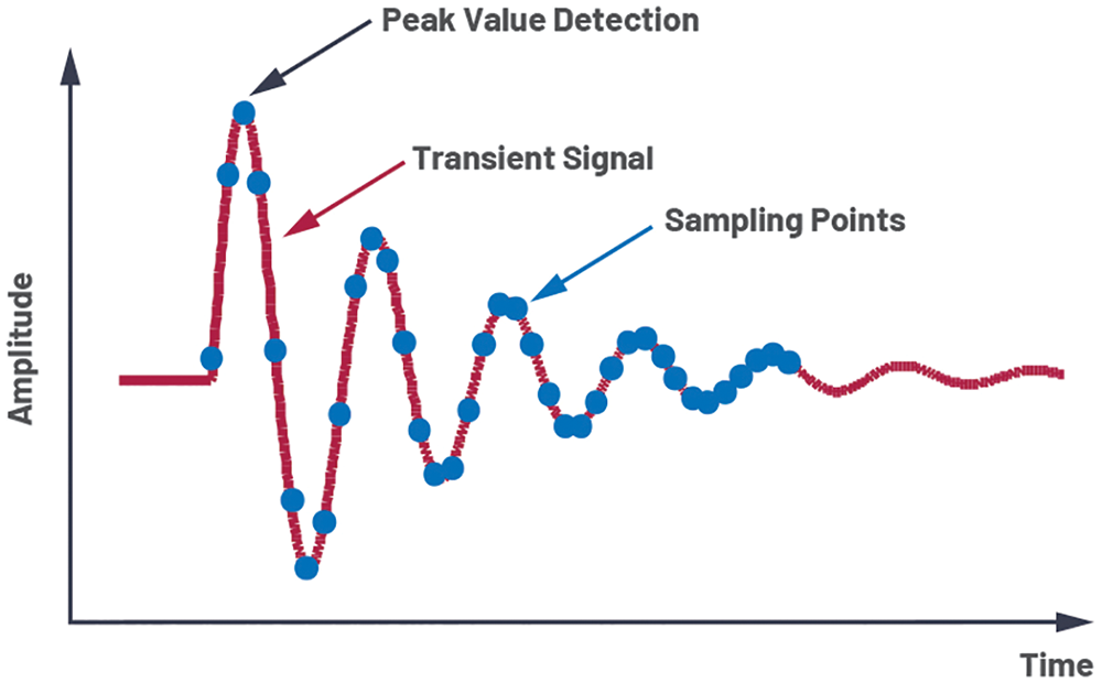 Figure 4. Oversampling is required for time domain peak value detection of a transient signal.
• Noise. As the noise contained in each sample can directly impact the amplitude detection accuracy of a time domain waveform, it is the total rms noise value that matters in the time domain analysis. The flatness of the noise spectral density isn’t important, as long as the total integrated noise over the effective noise bandwidth meets the required measurement accuracy. Noise improvement DSP techniques, such as FFT process gains, are no longer available in the time domain analysis.
• Step response. The measurement signal chain needs to have a good step response in order to properly replicate the profile of the transient signal input. This impacts the filter design and selection in the DAQ signal chain.
DAQ signal chain design examples
In this section, we will use two CM system DAQ signal chain examples to show how to translate system requirements into signal chain design.
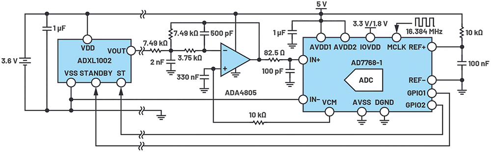
Example 1
System requirements
• 3 V; to 3,6 V battery-powered system in edge node architecture.
• Single-axis vibration sensing with ±50 G range.
• Support frequency analysis of up to 10 kHz; of (flat) bandwidth.
• Dynamic range >80 dB over 10 kHz; bandwidth.
• Support time domain analysis, including the shock pulse method, with sample rate of 128 kSps.
• Equal to or less than 0,1% of dynamic nonlinearity over full-scale range.
• Able to operate in a noisy environment and able to reject electromagnetic interference (EMI).
Sensor selection
An ADXL1002 MEMS accelerometer is chosen for the task of vibration sensing. It meets the key performance criteria and has the low power and small form factor that are well suited for edge node systems.
The ADXL1002 has a flat response bandwidth of 11 kHz, which is ideal for frequency analysis over the 10 kHz bandwidth of interest. The resonant frequency of the sensor is at 21 kHz. Signals at this frequency can be oversampled to support time domain analysis methods such as the shock pulse method.
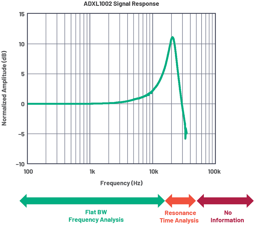 Figure 5. The ADXL1002 accelerometer’s frequency response divide.
The sensor has a noise density of 25 μG/√Hz up to 10 kHz. If the total rms noise over 10 kHz bandwidth is
The output of the ADXL1002 is a buffered voltage signal, with the amplitude proportional to both the sensed acceleration and the sensor’s supply voltage. The output signal is biased at a DC voltage that is equal to half of the sensor’s supply voltage. With a 5 V; supply, the ADXL1002 has a sensitivity of 40 mV/G. With a 3,3 V supply, the maximum sensor output signal swing over the ±50 G input range is
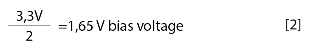
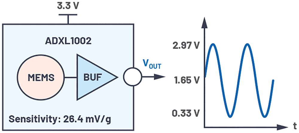 Figure 6. The full-scale output signal of the ADXL1002.
DAQ requirements
The DAQ signal chain to interface with the ADXL1002 sensor needs to meet the following requirements:
• Support the full output voltage range of the sensor.
• Have flat frequency response over 11 kHz.
• Able to oversample the resonant frequency by at least five times.
• Let the sensor dominate the overall AC and DC performance.
• Provide adequate aliasing rejection to signals outside the band of interest.
• Low power.
• Small solution size.
The proposed solution is shown in Figure 7. It consists of the single-channel precision sigma-delta ADC AD7768-1 and the ADC driver amplifier ADA4805-1.
ADC selection
The AD7768-1 is a versatile precision ADC that has many modes of operation, which allows the trade-off between power, bandwidth and noise. The programmable digital filter is essential for aliasing rejection and different filter types can be used to support frequency and time domain analyses.
In this design, we’ve chosen to operate the device with the following configuration:
• Enable integrated reference buffer on REF+ input.
• Low-power mode.
• Low-ripple wideband filter with 32 kSps ODR (filter option A).
• Sinc5 filter with 128 kSps ODR (filter option B).
The integrated reference buffer allows a very compact design and removes the need for an additional buffer amplifier. This design takes the advantage of the ratiometric relationship between the ADXL1002’s output to its supply voltage and the fact that the AD7768-1’s reference buffer supports rail-to-rail operation, by sharing the 3,3 V battery supply between the sensor and the ADC and using the same voltage as the ADC’s reference voltage. Not only does this remove the need to generate a dedicated reference voltage for the DAQ signal chain, it also removes any measurement signal magnitude variation due to a change in supply voltage, such as battery discharge over time.
The low-power mode operation minimises the power consumption of the ADC to maximise the battery life. In low-power mode, the AD7768-1 can support a brick wall-style, low-ripple wideband filter with 13 kHz of flat (–0,1 dB) bandwidth at ODR of 32 kSps (filter option A), which is perfect for covering the 11kHz flat bandwidth of the ADXL1002 to perform frequency analysis.
The brick wall filter has a nearly ideal filter profile and is great for frequency analysis, but the high-order filter makes it less desirable for performing time domain analysis. For this reason, the sinc5 filter, which has great step response, can be used to meet the need for time domain analysis.
The AD7768-1 in low-power mode with a sinc5 filter supports output data rates up to 128 kSps and -3 dB frequency at 26 kHz (filter option B), enough to oversample the sensor’s 21 kHz resonant frequency by more than five times. The digital filter type and the output data rate are all register-programmable through the SPI interface, which allows the signal bandwidth to be adjusted dynamically based on application needs.
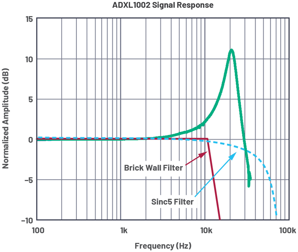 Figure 8. How different digital filter responses can be used for different measurement requirements.
Compared to sending the unfiltered oversampled data to an external digital host for postprocessing, the integrated digital filter on the AD7768-1 greatly improves the power efficiency of the digital processing. The power consumption of the AD7768-1 in low-power mode, with a 3,3 V supply on AVDD1, AVDD2 and IOVDD and reference buffer on REF+ pin enabled, is estimated to be 10,2 mW for a sinc5 filter with 128 kSps ODR and 12,6 mW for a wideband low-ripple filter with 32 kSps ODR.
The noise of the AD7768-1 in this configuration is 11,5 μV rms for filter option A and 49,5 μV rms for filter option B. The input signal to the ADC in this design is a pseudo differential signal of ±1,32 V. The effective dynamic range of the ADC with this input range and filter option A is
AFE design
Although the ADXL1002 has a buffered output, its output impedance is not low enough at the ADC’s sampling frequency (2,048 MHz) to fully settle the ADC’s input during sampling. A wide-bandwidth driver amplifier is recommended to bridge the sensor with the ADC. The ADA4805-1 is chosen for this task based on its characteristics of wide bandwidth, low output impedance, low noise, small size and low power consumption.
As the combined ADC and driver amplifier’s noise performance is below that of the sensor, there is no need to gain up the sensor’s output signal. The ADA4805-1 has rail-to-rail output but not rail-to-rail input. For this reason, the driver is configured as an inverting buffer with a gain of 1. The driver’s output headroom is verified to satisfy the full-scale signal swing.
The AD7768-1’s digital filter also has no rejection at the frequency band around the ADC’s sampling frequency. An active antialiasing filter is constructed with the ADA4805-1 to help the digital filter achieve adequate overall out-of-band signal rejection across frequency. The design is a second-order low-pass filter with multi-feedback architecture and a near Butterworth response, with a -3 dB corner at 32 Hz and -73 dB of rejection at 2 MHz.
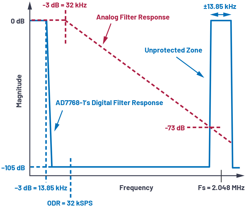 Figure 9. The overall filter responses of the Example 1 signal chain.
The resistor value used in the driver circuit is carefully chosen to balance between power consumption, circuit noise, capacitor size and DC offset error due to the input bias current of the ADA4805-1.
Overall performance of the combined signal chain is listed in Table 1.
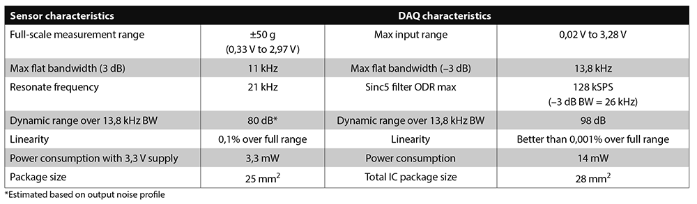 Table 1. Example 1 Sensor and DAQ characteristics.
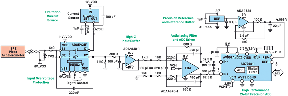
Example 2
System requirements
• DAQ module in DAQ centralised architecture with channel-to-channel isolation.
• Pseudo differential input with ±12 V maximum input range.
• Supports IEPE interface.
• AC and DC bias input options.
• Input overvoltage protection of up to ±60 V.
• 1 MΩ input impedance.
• Supports frequency analysis of up to 100 kHz of (flat) bandwidth.
• Dynamic range >105 dB over 100 kHz bandwidth.
• Alias free (able to reject all signals outside the band of interest by -105 dB).
• Supports time domain analysis, including shock pulse method.
• Total harmonic distortion is ≤-115 dB with 1 kHz full-scale input.
• High DC precision.
• Supports programmable filter bandwidth and output data rate.
The proposed solution is shown in Figure 10. It uses the same 24-bit, precision sigma-delta ADC (the AD7768-1) as Example 1. The analog front end consists of an ADG5421F input protection switch, an LT3092 constant current source for providing IEPE sensor supply current, an ADA4610-1 precision JFET buffer amplifier, an ADA4945-1 fully differential amplifier for ADC driving and the construction of an antialiasing filter. An ADR444 precision reference source is used to provide the reference to the ADC with the help of an ADA4528-1 precision op amp as the reference buffer.
Sensor supply
The IEPE interface is a two-wire interface, with the sensor output signal (voltage) and the sensor supply (current) sharing the same wire. An LT3092 is used to construct a low-noise 2,5 mA current source across the 30 V supply to power the sensor. The current value can be programmed via resistor value in order to support longer cable length/higher cable capacitance.
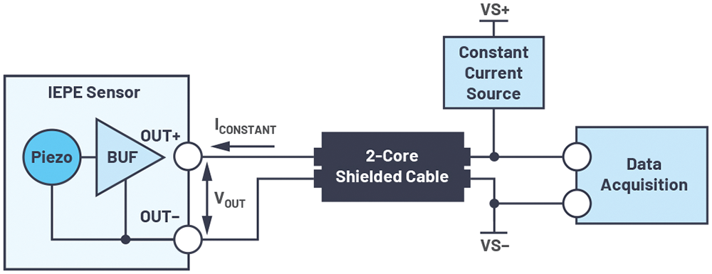 Figure 11. Only a 2-wire cable is needed to interface with the IEPE sensor.
Some IEPE sensors are not case isolated, meaning their OUT- terminal may be connected to the local ground. If the sensor-interfacing DAQ is also not isolated, then the DAQ also needs to be ground referenced. In this design, the DAQ channel is isolated. This helps remove the grounding and supply level constraints, allowing the DAQ to be designed with a bipolar supply to support more symmetrical bipolar input signals.
Input protection
An ADG5421F protection switch is employed to provide input overvoltage protection to the circuit. The internal switch opens when the input voltage exceeds the supply range to protect the rest of the DAQ signal chain. The ADG5421F can withstand up to ±60 V of input voltage and its low, stable RON is essential to minimise signal distortion.
In this design, this switch is also used to provide programmable options to the signal chain input configuration. Based on the switch configuration, the signal chain input can be configured as AC or DC coupled and the current source can be independently switched in and out.
An additional TVS is added with a small (10 Ω) series resistor to help improve the ESD protection of the input node.
ADC selection
The channel isolation requirement drives the need for a single-channel DAQ solution.
These two examples showcase the versatility of the AD7768-1. When operating in full-power mode, this ADC is capable of achieving 110 kHz of flat bandwidth with the brick wall digital filter
The AD7768-1 also has industry-leading dynamic linearity and DC performance. This includes having typical THD of -120 dB with a 1 kHz near full-scale sinusoidal input signal, 300 nV/°C offset error drift and 0,25 ppm of gain error drift.
For multichannel DAQ systems that do not require channel isolation, the quad (AD7768-4) or octal (AD7768) version of the same ADC can be used.
AFE design
The input signal needs to be buffered to achieve the required impedance. The buffer amplifier needs to have low input bias current, low noise, good dynamic linearity, high DC precision and adequate bandwidth. The ADA4610-1 JFET op-amp is selected based on these requirements. It is configured as a unity-gain buffer and requires a ±15 V supply.
The signal then needs to be attenuated and level shifted to fit within the input range of the ADC. It is desirable to convert the pseudo differential signal into a fully differential signal. This conversion improves the measurement dynamic range by 6 dB and greatly reduces the second harmonic distortion. The signal then needs to be filtered to reject aliasing and buffered with a high-bandwidth and low-output impedance ADC driver amplifier to ensure proper settling of the ADC input. Fortunately, all of these functions can be realised by a circuit design using a single ADA4945-1 fully differential ADC driver amplifier with minimum distortion and added noise while maintaining excellent DC precision.
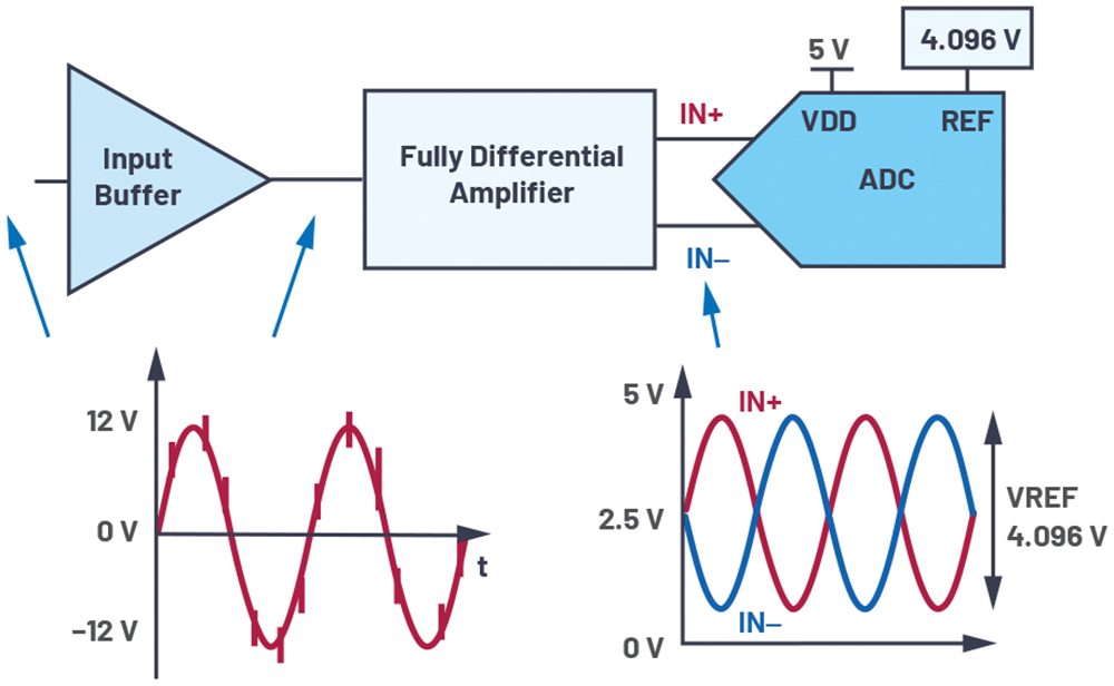 Figure 12. Signal conditioning in the analog front end.
In this circuit, the signal is attenuated by 0,33, which allows a
As described in Example 1, the AD7768-1’s digital filter also has no rejection at the frequency band around the ADC’s sampling frequency. In full-power mode, the ADC’s effective sampling frequency is at 16,384 MHz. An active antialiasing filter is constructed with the ADA4945-1 to help the digital filter achieve adequate overall out-of-band signal rejection across frequency. The design is a third-order low-pass filter with multi-feedback architecture and a near Butterworth response.
Another low-pass pole is added by an RC circuit in front of the ADA4610-1 buffer amplifier to help further increase the aliasing rejection at full scale. The overall signal chain frequency response has a -3 dB corner at 440 kHz to minimise the magnitude and phase distortion to the in-band response. The magnitude droop caused by the antialiasing filter at 100 kHz is less than 10 mdB. The magnitude response at 16,3 MHz is around -108 dB. This, combined with the brick wall digital filter of the AD7768-1, produces an alias free signal chain that is capable of rejecting all out-of-band signals by at least 105 dB.
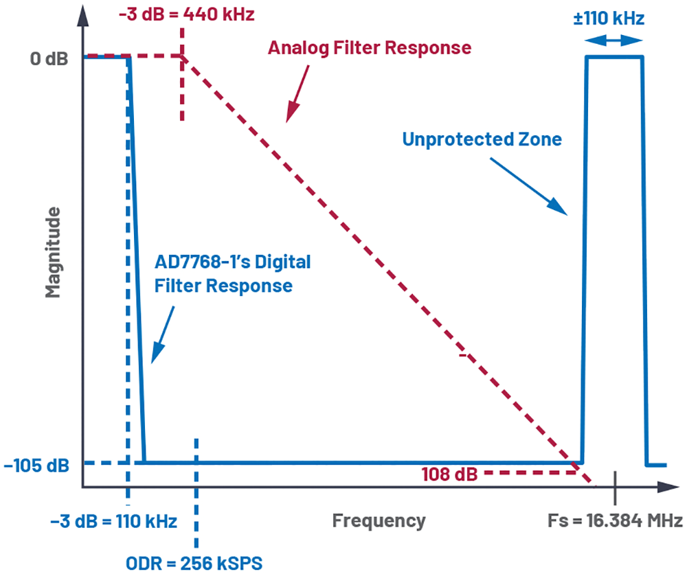 Figure 13. The overall filter responses of the Example 2 signal chain.
Isolation and power management
The digital and power isolation and power management solution will not be discussed in detail here. Solutions such as the ADP1031 can provide an SPI interface plus ±15 V and 5 V supply voltage across isolation. An ADuM140D high-speed digital isolator can be used to provide MCLK and SYNC_IN signals across isolation for across-channel sample synchronisation.
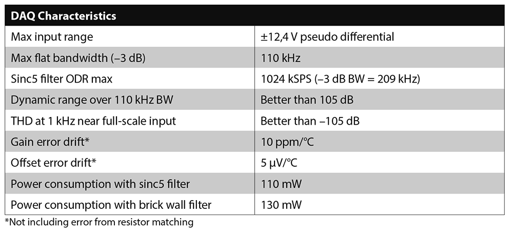 Table 2. Example 2 DAQ characteristics.
Summary
In conclusion, this article has detailed how the choice of system architecture, sensor type and analysis methods can dramatically impact the DAQ signal chain design in a condition monitoring system. The design considerations discussed here, along with the example reference designs, will hopefully help system designers make the best design choices for their condition monitoring systems.
To learn more about Analog Devices’ condition-based monitoring system-level solutions, visit www.analog.com/cbm.
| Tel: | +27 11 923 9600 |
| Email: | [email protected] |
| www: | www.altronarrow.com |
| Articles: | More information and articles about Altron Arrow |


© Technews Publishing (Pty) Ltd | All Rights Reserved
 printer friendly version