


Panasonic’s Industrial Solutions Company has commercialised a semiconductor package substrate material (which it calls R-1515V) that enables both low package warpage and high assembly-level reliability. The newly developed material has very low thermal expansion properties to reduce warping of the substrate during the packaging process and optimised mechanical properties designed to lower the residual stress on solder joints created during reflow assembly.
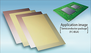
Semiconductors, the cornerstone of modern electronics, are critical to the advancement of IoT, AI, V2X, 5G and other leading-edge technologies. These devices have continued to improve and evolve in both die performance and packaging designs over time. The current generation of advanced package designs exhibit a relatively large footprint, a plethora of I/Os and high-density interconnecting structures like those found in 2.5D packages. Along with the operating performance improvements, most industrial and commercial applications demand high assembly-level reliability from the assembled packages.
Panasonic has successfully developed many types of products for motherboard material and semiconductor packaging and assembly over the years, including semiconductor package substrates, semiconductor encapsulation materials and assembly-level reinforcement materials.
Improving chip packaging reliability requires reducing the substrate warpage during packaging, i.e., mounting chips on the IC substrate followed by an encapsulation process. In addition, the stress imparted to the solder balls during the reflow assembly process – during which the semiconductor package is assembled onto a motherboard – needs to be lowered to ensure long-term operational reliability.
The coefficient of thermal expansion (CTE) of this new substrate material is much closer to that of silicon IC chips, reducing warpage caused by the thermal excursions experienced during packaging processes. In addition, the new substrate material features excellent thickness tolerances, ensuring stable junctions between the substrate and the ICs, further improving the reliability of packaged chips. The modified flexibility and buffering properties of the new material alleviate the stress on solder balls, improving the assembly-level reliability.
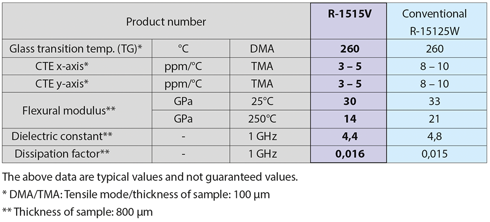 Comparative performance characteristics of the new substrate material.
R1515V has the following features:
1. Low thermal expansion coefficient (CTE) – close to that of silicon IC chips – reduces warping and addresses a critical challenge with the IC chip packaging process. By using the resin design expertise honed over decades of electronic circuit board materials development, Panasonic has developed a material with a low thermal expansion coefficient of 4 ppm (measured by the company), close to the thermal expansion coefficient of semiconductor ICs. This reduces warping caused by the difference in CTE between the substrate and the ICs and improves the reliability of mounting the chips on the substrate.
2. A combination of flexibility and buffering features, while retaining low thermal expansion properties through a stress relaxation technology, improves the reliability of the assembly process. Based on simulation of modelling results, Panasonic developed a material combining flexibility and buffering properties by using internally developed resin design technology, while retaining low thermal expansion properties. This material absorbs and disperses the residual stress on the solder balls between the semiconductor package and the motherboard, which improves the reliability of SMT assembly without affecting the quality of IC packaging.
3. Excellent thickness tolerances to ensure stable junctions between the substrate (core material) and the IC, which further improves the reliability of IC packages. With its precision resin flow control technology, which was established over decades of circuit board materials development, Panasonic has succeeded in ensuring laminated mouldability while controlling resin flows, resulting in minimal thickness variations. This makes junctions between the substrate (core material) and the IC stable, further improving the reliability of IC packaging.






© Technews Publishing (Pty) Ltd | All Rights Reserved
 printer friendly version