


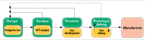
The popularity of BGA and CSP packaging has accelerated the adoption of JTAG boundary scan, leading to a new paradigm of concurrent design, analysis, simulation, debug and test. Design engineers can now not only build manufacturing test systems, but also compress product design cycles by exploiting the natural synergies throughout the design cycle.
Introduced around the year 2000, BGA (ball grid array) and later CSP (chip scale package) have rapidly become the dominant packaging technology for advanced products. Because traditional test methods like ‘bed-of nails’ or ‘flying probe’ cannot physically access the solder balls underneath such packages, this has greatly accelerated the adoption of JTAG boundary scan as the only available test solution.
With JTAG boundary scan test methodology, not only is the capital cost of implementing a test solution lower but the cost resides more in the required software tools than in the scan hardware itself. Where, historically, high capital cost of traditional ATE hardware meant that design and test engineering functions were separated (physically and in terms of personnel), JTAG fits perfectly with the trend towards smaller teams that are organised around projects, not organised according to ‘design’ or ‘test’ specialism.
The same engineers will work on aspects of both design and test, bringing significant benefits, such as better design for test (DFT), more efficient debug, reduced board spins and higher test coverage in production.
Design and test parallelism
At earlier stages in the evolution of our industry, there were often design engineers who had little input as to the design of the test solution, and test engineers who had to find ways to test hardware already designed, without the opportunity to optimise the possible test coverage at the design stage.
XJTAG has pioneered the concept of a common tool suite that creates value at multiple points in both the design and the test work flows, and therefore enables and encourages concurrent development from an early stage in a project. XJTAG promotes this way of working as a template for the future.
Flexible design and manufacturing
At the heart of the XJTAG system is XJEase, a dedicated JTAG programming language. Because the syntax is very similar to other high-level languages, it is very quick to learn, has all the facilities of a high-level language (like loop constructs and syntax and data type checking) but at the same time has powerful features targeted at JTAG test, for example the ability to handle bit fields of unlimited width and scan-specific instructions.
Traditional ATE test systems were based on the concept of test vectors and a simple PASS/FAIL operation. Test vectors (strings of 1s and 0s) represent test values at the lowest level of abstraction.
Therefore – just like comparing microprocessor assembler code with a high-level programming language – there is a big maintenance overhead whenever any changes are made and it is very easy to introduce errors. Test modules developed for one product are not easily portable to the next generation product, even though many of the same devices may be retained.
XJTAG pioneered the concept of device-centric testing which is analogous to object-oriented programming. Once a test module is written, it can be inserted into many designs; the XJTAG system takes care of the external references.
XJTAG design and test vision
The guiding vision at XJTAG is to make each detail of the design available to share and elaborate in its different design views at the very earliest stage in the design cycle. XJTAG aims to be more than a standalone test tool, but rather a whole environment that enables users to plan and visualise the test solution so that when the first prototype boards arrive, they are totally familiar with the test approach and already have much of the code written to start debugging.
The concurrent design and test development flow that XJTAG champions has many benefits in raising overall productivity within the team. Design engineering has early exposure to the XJTAG environment, and incorporates DFT features at an earlier stage in the design process. DFT and DFT analysis is at a more advanced stage earlier in the project. DFT additions, to further increase fault coverage, can be specified at an earlier stage, when the cost to make changes is much lower.
Often XJTAG users report that they have found design errors that saved a board re-spin because errors that prevent successful test program operation can be overlooked from the design engineering perspective, even though they are critical errors. It is also possible for such errors to impact mission mode operation in some way, so that prototype debug becomes impossible.
XJTAG has its own formalism which is distinct from other checking methods that engineers use, like simulation or modelling. As engineers work through the XJTAG setup processes, they will not be allowed to proceed unless that formalism is satisfied.
It thus acts like a further checking round and that can be very valuable. After all, it only takes one error in an unfortunate location to make a prototype board unusable, or at least delay board bring-up while a workaround is found.
Time-to-market pressures
In the modern electronics era, product lifecycles are compressed in time, so a major focus at XJTAG is finding ways to make the test program development faster and easier. An intelligent text matching algorithm automatically matches parts listed in BOM (bill of materials) to parts in an integrated test library.
In this way, most of the board setup is automated, with the design or test engineer needing to intervene only to resolve corner cases. A carefully thought out GUI guides engineers through the setup stages to maximise productivity. Critically, XJTAG Developer is designed to allow DFT analysis at the earliest possible stage in the design and test evolution.
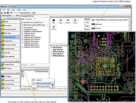
Visualisation aids
The XJTAG Development System includes a Layout Viewer as standard to work with ODB++ so that, as soon as board layouts are available, test nets can be viewed physically as well as in netlist and schematic view. The layout viewer is an even bigger benefit during production testing: as soon as a fault is detected during the boundary scan testing, the nets involved in the failure can be displayed instantly on the screen so that the test operator can see the most likely location of the fault.
Higher quality is its own reward
Anthony Merry, chief technical officer at Haliplex (an existing XJTAG customer) explains how the company has benefited from XJTAG’s methodology: “We have reduced the typical time to commission a new design by around four days. Given the number of new boards we develop in a year, this saves us around $24 000 of engineers’ time.
“In production, the superior diagnostic capabilities of our boundary scan test system allow our manufacturing partner to identify and repair faults themselves, rather than adding them to our ‘repair pile’. As a result, the number of failed boards sent to us has reduced by around 90%. This is saving over $64 000 of waste per year as well as around $12 000 of our repair technicians’ time.”
XJTAG’s Simon Payne and David Baxter will be in South Africa next month to present at a series of workshops hosted by ASIC Design Services. See 'Events' for details on when and where they are taking place and how to register.
Background to boundary scan
Boundary scan uses dedicated test circuitry implemented on-chip in many components – particularly microcontrollers or FPGAs. Each device provides its own test access port, which is connected to a serial boundary-scan chain at the board level leading to a single four-pin header at the board edge. The test equipment is connected to the header, and no access to individual component I/O pins is required.
This test technique, first proposed by the Joint Test Action Group (JTAG), was ratified as the standard IEEE 1149.1 in 1990. The XJTAG test system maximises the potential for boundary scan testing by including features to streamline test generation and promote test re-use, and by taking advantage of available board-level connections including I²C or SPI buses to test non-JTAG components not directly connected to the boundary-scan chain.
This now allows a wide range of components such as memories, Ethernet ports, ADCs and DACs to be tested from within the boundary scan environment. Other devices such as sensors, display drivers and switches are also all within reach.
| Tel: | +27 11 315 8316 |
| Email: | [email protected] |
| www: | www.asic.co.za |
| Articles: | More information and articles about ASIC Design Services |


© Technews Publishing (Pty) Ltd | All Rights Reserved
 printer friendly version