Four reasons for X-ray inspection of surface mount devices
25 February 2015
Manufacturing / Production Technology, Hardware & Services
Vision inspection systems can find visible defects on PCBs, but these systems can only check the surface for errors, not the hidden solder joints of components like BGAs and flip chips. X-ray inspection can provide critical verification of the integrity of hidden solder joints on surface-mount devices.
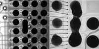
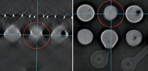
Figure 1. Solder ball shorts.
The following are four of the most common examples of faults that X-ray inspection is best suited to detecting.
1. Solder ball shorts
Solder ball shorts, or solder bridges, can be easily detected with an X-ray image, as shown in Figure 1.
2. Solder ball voids
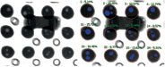
Figure 2. BGA void image with auto void calculation.
Ball-void inspection is used for BGA/CSP inspection along with solder ball bridge inspection.
Modern X-ray inspection systems can perform auto ball-void calculations (Figure 2).
Figure 3. BGA void location.
Not only is the size of the BGA voiding area important, the location of the BGA void is also important (see Figure 3), especially if the voiding area is close to the PCB pad area, because there is a possibility that this voiding area could cause a micro-crack.
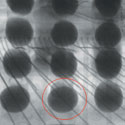
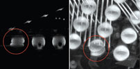
Figure 4. Solder ball open.
3. Solder ball open / micro cold solder
Solder ball attachment to the PCB pad is a critical inspection criterion. A high-resolution and high-magnification X-ray inspection system is required to detect a solder ball open defect. The X-ray image in Figure 4 shows a solder-ball open where the copper pad is separated below the solder ball.
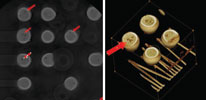
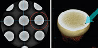
Figure 5. Solder ball open caused by small solder ball.
3D CT can assist with clear visualisation of open patterns. Figure 5 shows a solder ball open caused by the solder ball being too small. The image on the left shows a Y-Z slice image, indicating that the solder ball is smaller than the other ones. The image on the right shows an X-Y slice, indicating that the PCB pad (dark area) is not surrounded by a solder ball (white edges).
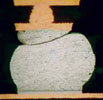
Figure 6. Cold solder – optical image.
Micro cold-solder joints can also be visualised with 3D CT, as illustrated in Figures 6 and 7.
Figure 7. Cold solder – non-destructive 3D CT image.
4. Solder ball crack
Using oblique CT technology, a solder ball crack can be visualised. Figure 8 shows a 10 micron solder ball crack.
Figure 8. Solder ball crack.
For more information contact Igmar Grewar, Quamba Technologies, +27 (0)83 417 4294, [email protected], www.quamba.co.za
Further reading:
World-first 016008 mm component placement
Manufacturing / Production Technology, Hardware & Services
Fuji has achieved the world’s first placement of 016008 mm (0,16 x 0,08 mm or 006 x 003 inches) size components on printed circuit boards with its SMT pick and place machine, NXTR.
Read more...
Lifecycle and obsolescence: Protecting electronics through process
Production Logix
Manufacturing / Production Technology, Hardware & Services
At Production Logix, we believe longevity is not accidental. It is engineered through early visibility, structured response, and disciplined execution, in partnership with our OEM customers.
Read more...
Maximising squeegee quality and durability
Testerion
Manufacturing / Production Technology, Hardware & Services
Transition Automation has announced two new product advancements designed to improve SMT printing performance and extend squeegee life: laser-enhanced Permalex bonding and integrated edge protectors.
Read more...
NeoDen ND2 PCB screen printer
ZETECH ONE
Manufacturing / Production Technology, Hardware & Services
The NeoDen ND2 PCB screen printing machine is a fully automatic stencil printer designed to deliver precise and consistent solder paste application in modern SMT production environments.
Read more...
Understanding the BGA rework process
Techmet
Manufacturing / Production Technology, Hardware & Services
BGA rework is a highly technical process that involves removing the faulty component, preparing the circuit board, and installing a new or repaired device, while maintaining the integrity of the printed circuit board.
Read more...
Flexible three-process reflow soldering system
Truth Electronic Manufacturing
Manufacturing / Production Technology, Hardware & Services
By combining multiple soldering technologies within a single system, the Vision TripleX system enables manufacturers to adapt easily to different assembly requirements, board designs, and production volumes.
Read more...
Inline vapour phase soldering for high-volume production
MyKay Tronics
Manufacturing / Production Technology, Hardware & Services
The VP2200-100 vacuum inline vapour phase soldering system from ASSCON is designed for fully automated, high-volume electronics manufacturing where process consistency and solder joint quality are critical.
Read more...
Global electronics solutions since 1964
IMP Electronics Solutions
Manufacturing / Production Technology, Hardware & Services
Over more than six decades, IMP Electronics Solutions has built a reputation for technical expertise, reliable supply chains, and strong partnerships with both customers and manufacturing partners.
Read more...
Driving excellence in electronics manufacturing
Jemstech
Editor's Choice Manufacturing / Production Technology, Hardware & Services
Jemstech’s reputation for disciplined execution and client-focused service has earned it strong loyalty from companies operating in demanding industries.
Read more...
When do you need Nitrogen in reflow?
Truth Electronic Manufacturing
Manufacturing / Production Technology, Hardware & Services
Nitrogen in reflow soldering is often seen as a performance enhancer, offering improved wetting, shinier joints, and fewer defects. But it is not always necessary.
Read more...


 printer friendly version