


Current transducers in which isolation is required generally detect the magnetic field of the measured current; this has the additional advantage of allowing both AC and DC currents to be measured. There have been two aspects to the trend in LEM open-loop current transducers in recent years: cost and size have been continuously reduced, and by using custom proprietary CMOS ASICs as the sensing element the performance parameters such as accuracy and response time approach those of more complex closed-loop transducers.
Usually the ASIC is placed in the air gap of a small magnetic circuit which gives noise-free amplification of the field and screening from external interference. Most of LEM’s conventional open loop transducers measure currents in the range of 3 A to hundreds of Amps, isolation levels are up to 8 kV and the response time from 2 μs.
Some applications, particularly for motor drives, have the same need for speed but are less demanding of the current range and isolation levels while having strong pressure on price. In applications such as for example white goods, window shutters and air-conditioning, low cost and small size are particularly important. For these cases LEM has now introduced an additional family of sensors, the ‘GO’ family, whose size is reduced even further by eliminating the magnetic circuit. Instead, the primary current is passed directly into a standard integrated circuit package where its magnetic field is measured by a new ASIC derived from that used in conventional transducers.
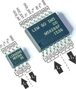
Figure 1 shows two such examples. One is in an SOIC-8 package and the four secondary-side pins are for the supplies, the output voltage Vout and a reference voltage Vref. The other is in an SOIC-16 package where eight secondary pins are available so the opportunity has been taken to provide two different over-current detect (OCD) warning levels; one very fast, and the other slower but more accurate. The speed and accuracy of the GO transducers are very similar to those of a transducer with a magnetic circuit. The absence of a magnetic circuit of course means that there is zero magnetic offset.
Architecture and features
The GO transducer ASIC is derived from that used in LEM open-loop transducers which have a magnetic circuit. There is considerable production experience with this ASIC, which has allowed introduction of some extra features around the well-known signal path blocks. In this section the design of the GO transducer is described and some contrasts are made with magnetic circuit transducers.
Figure 2 shows a simplified block diagram of a GO transducer in a 16-pin package. Multiple Hall cells implanted in the ASIC are placed on both sides of the primary current to detect its magnetic field. Their offset, together with that of the input amplifiers, is eliminated with chopping techniques which modulate the Hall cell output to an AC signal. After amplification the Hall signal is demodulated back to its original frequency before buffering and filtering at the output. The fast response time is achieved by using a high chopping frequency and internal filters which reduce the noise bandwidth of the system.
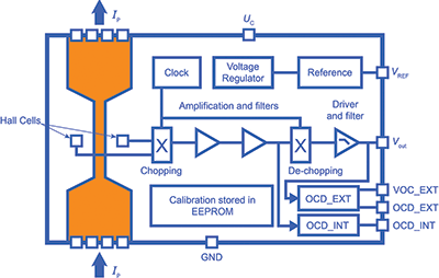
During production each transducer is individually calibrated. Tests are done at three temperatures; the drifts of sensitivity and output offset are measured and corrections stored in an EEPROM memory on the ASIC. This ensures that the transducer accuracy is maintained over temperature and ageing.
The ASIC is separated from the primary conductor by a series of insulating layers – an optimum separation has been chosen for the best compromise between highest isolation with a wide separation and highest magnetic field at the Hall cells with lower separation. The Hall cells on opposite sides of the primary are sensitive to fields in opposite directions so the transducer is immune to uniform magnetic fields from sources other than the measured current. The exact lateral position of the Hall cells relative to the primary is not critical, since the difference between the outputs of the cells on the opposite sides is used. In other words, the Hall cells are configured as a gradient sensor.
The detail of the OCD implementation is shown in Figure 3. The aim is to give two different levels of warning. The first level is for currents slightly higher than expected, to warn for example that a drive current is going out of the expected range. This OCD needs to be reasonably accurate, not especially fast, and each user may want to set a different level. The relaxed speed requirement allows the input to this first OCD to be taken from the transducer output, and the level is set by user-chosen external resistors, hence its name, OCD_EXT.
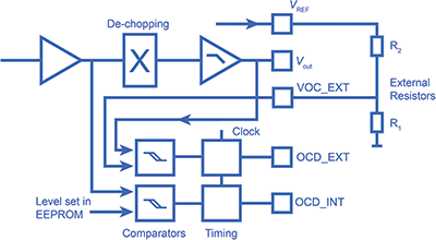
The second level is intended to warn of currents which are dangerously high, due to a short circuit for example. The response time must be extremely fast, but the value and accuracy of the detection level are not critical. To obtain a fast response time and to allow an OCD level outside the normal linear operating range the input to the second OCD is taken before the demodulation block. Its level is set internally by storing a parameter internally in the EEPROM – so it is known as OCD_INT. The level is typically set at 3x the nominal primary current, IPN. Note: Figure 3 is slightly simplified in that it omits the detail that ensures that both OCDs respond to both positive and negative over-currents.
Both OCDs check that the over-current condition is present for at least 1 μs approximately, to avoid false alarms, and both outputs, once triggered, are maintained for 10 μs to be sure that the condition can be detected. The outputs are open-drain, which conveniently allows OCDs from several transducers to be connected together. OCD_INT triggers in less than 2,1 μs; the typical response time of OCD_EXT is 10 μs.
The footprint of a GO series transducer in a 16-pin package is about 100 mm², and in an 8-pin package it is half of this. The corresponding value for the smallest PCB-mounted transducer with a magnetic circuit is about 400 mm². The heights are 2,5 mm and 12 mm respectively. However, for both types, in the higher current ranges some allowance must be made for dissipation of the heat generated in the transducer primary, which is greater in the GO series since the primary resistance is higher.
Key parameters and measured transducer performance
In Table 1 some of the key electrical parameters of the GO series transducers are presented. For comparison, the values of the same parameters for a small open-loop transducer with a magnetic circuit are also given – a small transducer has been chosen to give the most meaningful comparison, a larger transducer would have different parameter values.
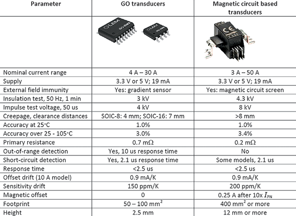
Table 1 shows that many key electrical parameters have been inherited unchanged or slightly improved from the established sensors with a magnetic circuit, whereas others, such as size and insulation, are different, allowing the two transducer families to address quite different markets.
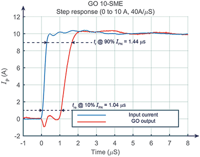
Figure 4 shows a measured response time after a primary current change in 0,3 μs. The compact size and absence of magnetic components in the transducer gives a response with very little overshoot and ringing.
The assertion made previously that the GO transducers are not disturbed by external magnetic field will be true if the amplified electrical output of the Hall cells from both sides is the same, since the difference between the two outputs is used. To satisfy this condition, (i) the sensitivity of the Hall cells on both sides of the primary (and the amplifiers to which they are connected) must be the same; that is, they must be well matched; (ii) the magnetic field must be the same on both sides of the primary; it must be uniform.
Considering point (i), because the Hall cells and the amplifiers are made with large devices, their matching is excellent. When a uniform external magnetic field is applied to a GO transducer it is almost perfectly rejected. However, for point (ii) the magnetic fields generated by conductors placed close to the transducer are not uniform and the outputs from the two sides of the primary will not be perfectly rejected. This has been investigated for conductors placed in four different positions near a GO transducer; see Figure 5.
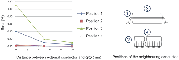
The worst case is position three in which the external conductor is aligned with the GO primary. If the external conductor carries 10 A and the measured current is also 10 A the transducer output error due to the external current will be only about 1% of the measured current, even with zero distance between the external conductor and the GO. This investigation shows that with a minimum of care in the design of PCB layout, external conductors will have negligible influence on the accuracy of GO series transducers.
Another important consideration in miniature transducers is the effect of a sudden primary voltage change on the transducer output. This is best handled at the ASIC level. Where internal signal levels are small they are always differential, and changes in their common mode level due to an external transient have little effect.
Sensitive nodes can be protected by small grounded screens on the top metal layer. Screening is used only over the small areas where it is needed. This has many advantages over large screens: the top metal layer remains available for interconnect where screens are not needed; the ASIC die is not hidden and damaged parts can be analysed; and there are no Eddy currents which would slow the response time.
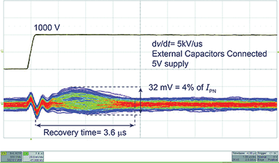
Figure 6 shows the effect of a dv/dt of 5 kV/μs on the output of a 25 A GO (GO 25-SMS). The peak disturbance on the output is 4% of IPN and the recovery time is about 3,6 μs.
| Tel: | +27 11 626 2023 |
| Email: | [email protected] |
| www: | www.denver-tech.co.za |
| Articles: | More information and articles about Denver Technical Products |


© Technews Publishing (Pty) Ltd | All Rights Reserved
 printer friendly version