


SiC (silicon carbide) MOSFET-based power switches offer significant system advantages in terms of power density, efficiency and cooling effort due to their much lower losses compared to silicon IGBTs. It has been shown that the system costs of solar applications as well as the running costs of UPS systems can be drastically reduced despite the more expensive semiconductor component. Thus, the technology is ready to penetrate more and more applications in the coming years.
While the electrical performance of commercially available SiC devices is already outstanding, there are still concerns about SiC MOSFET reliability. Currently most of the parts on the market are based on a planar DMOS like design. In order to mitigate the very low conductivity of the planar channel the devices are operated for full turn-on at high gate oxide fields (using comparably thin gate oxides). Thus, special care needs to be taken particularly about the potential high field failure rate as a consequence of the quite high permanent on-state gate oxide stress fields of above 4 MV/cm. The dilemma between performance and robustness can be overcome with the trench concept introduced by Infineon.
The CoolSiC MOSFET uses a trench structure showing commonly significantly higher channel conductivities due to less defects compared to the planar channel on the so called Si face of 4H-SiC. An investigation of different orientations of the trench sidewalls resulted in slightly different threshold voltages as well as significantly different channel mobility. In Infineon’s device the most favourable orientation with respect to the highest possible channel conductivity was chosen for the MOS channel.
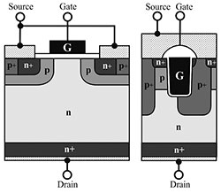
Figure 1 shows a sketch of the CoolSiC MOSFET cell. Following the considerations presented before, the doped regions adjoining the trench are asymmetric. The left hand side of the trench sidewall contains the MOS channel which is aligned to the so called a-plane of 4H SiC. A large portion of the bottom of the trench is embedded into a p-type region which extends below the bottom of the trench which also acts as a p-type emitter of the incorporated freewheeling body diode.
This MOSFET structure inherently exhibits a favourable capacitance ratio. The Miller capacitance CGD is small while CGS is comparably large. This allows for a well-controlled switching with very low dynamic losses. In particular this feature is essential to suppress undesirable parasitic turn-on.
A decisive criterion to ensure gate oxide reliability of SiC MOSFETs is the limitation of the gate oxide field in order to guarantee a sufficient lifetime and FIT rate. For SiC trench MOS structures in blocking state additional care has to be taken since the electric field in the trench corners is enhanced due to the trench shape. With respect to this specific cell configuration the field peak is found in the left trench corners. This local maximum of the electric field determines the lifetime of the gate oxide in blocking state.
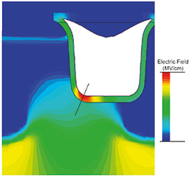
Figure 2 presents a 2D simulation result for the electric field under worst case conditions, i.e. at maximum drain source voltage of VDSS = 1200 V and a minimum gate voltage of VGS = -10 V. The simulation indicates that the electric field in the gate oxide can be limited to a value sufficiently low not to conflict with gate oxide lifetime requirements.
The typical on-resistance for the single chip device is 45 mΩ at VGS = +15 V, ID = 20 A and T = 25°C. The threshold voltage (typically 4,5 V) is significantly higher than for planar SiC MOSFETs, thus the part can be operated liked common IGBTs.
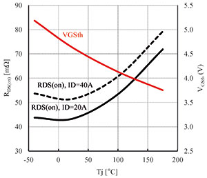
The temperature dependency of the on-resistance and threshold voltage is plotted in Figure 3 within the specified temperature range between -40°C and 175°C. The on-resistance has its minimum at room temperature and increases from RDSon = 45 mΩ to typically 72 mΩ at 175°C. This represents the physically expected resistance increase with temperature of a MOSFET with a low defect density in the channel region.
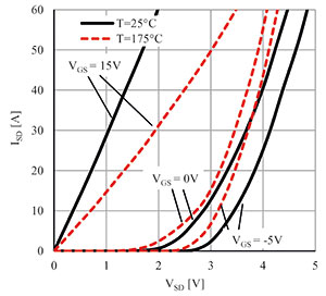
The characteristics of the 3rd quadrant are given in Figure 4. As pointed out before the MOSFET contains a body diode which can be used for hard commutation. Thus, it is not necessary to add an external and expensive additional SiC diode for freewheeling operation.
The curves with a gate source voltage of VGS = -5 V represent pure body diode operation without a partial bypass by the MOS channel. At zero gate voltage there is already some contribution of the channel to the current which lowers the source drain voltage VSD. However, very low VSD and linear characteristics are found as soon as the channel is turned on by applying +15 V to the gate. Now the corresponding 3rd quadrant on-resistance falls down to 33 mΩ at 25°C and 57 mΩ at 175°C, respectively. These values are lower compared to the 1st quadrant since the JFET resistance is reduced due to a negative feedback effect on the pn-junction bias. In order to keep static losses in diode mode low, synchronous rectification with an appropriate interlock time is recommended.
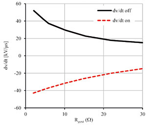
An essential feature of the MOSFET is that the voltage slope for turn-on as well as for turn-off is fully controllable by the external gate resistor in order to cope with any dv/dt limitations required by the system. Figure 5 proves that the voltage slopes dv/dt for turn-off and turn-on can be easily adjusted by the external gate resistor Rgext. The switching losses are almost invariant to temperature as long as the gate resistor is kept constant. This behaviour is in contrast to that of an IGBT since minority carriers do not impact the device behaviour in the MOSFETs.
The dynamic behaviour is mainly governed by the capacitances of the MOS system or by the built-up space charge regions. Both are in first order not dependent on temperature. In half-bridge configuration the body diode is active and shows an increasing impact with larger load current as well as higher temperatures. Obviously this is an effect due to minority carriers injected by the forward biased pn-junction which generates a reverse recovery charge. However, the absolute values at the rated current of 20 A are still reasonably small compared to the situation known from bipolar silicon devices and thus, will have just a minor impact on the total loss balance.
One of the most serious concerns about commercial SiC MOSFETs is the reliability of the gate oxide which is impacted by extrinsic defects. The root cause for extrinsic defects in the gate oxide of SiC MOS devices is dominated by the substrate material, the epitaxial process, and by defects of the remaining process chain. Hence, the challenge with respect to the gate oxide reliability of SiC MOS devices is how to ensure a low enough failure rate including extrinsic defects for a desired lifetime under given operation conditions, e.g. <1 FIT in 20 years for industrial applications.
In contrast to the misleading reports of oxide reliability at high reverse bias, which do not address the real challenge of SiC MOSFETs for practical applications, long-time gate stress tests in on-state were performed with a large number of devices in order to determine the extrinsic gate oxide failure rates under real operating conditions.
The investigation was done for two groups consisting of 1000 discrete devices. The tests were performed at 150°C under constant gate bias stress for 3 times 100 days each. The gate source voltage was increased by +5 V after each 100 days. The time stamp of each failure was monitored.
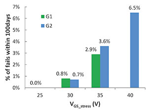
Figure 6 shows the sum of fails after each 100 day sequence. In the case of group G1 (green bars in Figure 6), the test started at a gate source voltage of +25 V with zero fails after 100 days. The test of group G1 ended at +35 V, which is +20 V above the recommended use voltage of +15 V, with a total of 2,9% fails after 300 days. The 2nd group (blue bars in Figure 6) started at 30 V, continued at 35 V and ended at 40 V, with 6,5% fails in total.
As could be demonstrated, these failure statistics fit well to the linear E-Model. By extrapolating this result to a lifetime of 20 years of device operation, the model predicts a failure rate of 0,2 ppm. This experiment demonstrates an IGBT-like reliability of the gate oxide with a failure rate under use conditions which is well below the typical industrial requirement specification of 1 FIT per die.
In addition, high temperature gate stress tests (HTGS) were performed. Both positive bias temperature stress (PBTI) as well as negative bias stress (NBTI) show well predictable power-law-like threshold voltage shifts of the form ΔVGSth ~ (time)n which is similar to silicon MOSFETs. Within 1000 hours stress time at 150°C, the total threshold voltage shift reaches about +0,3 V for VGS = +20 V and -0,1 V for VGS = -10 V.
Differently to silicon, the BTI induced threshold voltage shift in SiC MOSFETs is superimposed by a fully recoverable on-off hysteresis. This threshold voltage hysteresis is an intrinsic non-destructive feature of the SiC/SiO2 interface and occurs most likely due to very fast charge trapping at interface defects.
From an application point of view, the more relevant permanent or slowly recoverable threshold voltage shift component is limited to some 100 mV for typical DC stress conditions (1000 h/+20 V/150°C). The remaining threshold voltage shift at the end of the BTI stress test is most likely due to charge trapping at defects within the gate oxide close to the SiC/SiO2 interface. A carrier trapped at such a site does not degrade the oxide integrity but needs more time to be released.
For more information contact Davis Moodley, Infineon Technologies, +27 (0)11 706 6099, [email protected], www.infineon.com


© Technews Publishing (Pty) Ltd | All Rights Reserved
 printer friendly version