


Electronic devices have always been susceptible to damage from electrostatic discharge (ESD) or other over-voltage events.
Unfortunately, today’s electronic products have even less tolerance for DC voltages higher than 3,3 V, so an ESD pulse can prove catastrophic.
Various factors contribute to this reduced voltage tolerance, including the smaller manufacturing geometries of today’s most advanced integrated circuit chips. The level of on-chip circuit protection has also declined.
Perhaps the most significant factor is the tremendous popularity of mobile and portable devices like tablets, smartphones, digital cameras, MP3 players, etc. The nature of these mobile devices means they are used ‘on the go’ in uncontrolled and possibly static-filled environments, with only onboard circuit protection safeguarding them from an unexpected zap of ESD. Ensuring device longevity demands careful selection and placement of appropriate ESD protection devices on the printed circuit board (PCB).
The main purpose of ESD protection is to provide the lowest resistance shunt path to ground during over-voltage events or any transients. Proper PCB layout and routing of traces is critical to effectively using ESD suppression devices. Even the most ideal protection solution can be rendered useless if the proper layout techniques aren’t used.
Perhaps the most common type of location error among new circuit designers is placing the ESD protection device ‘wherever it fits’ on the board on the bus or data line to be protected, rather than taking the time to reorganise the board layout to allow placement of the device right at the port that’s subject to ESD or electrical overstress conditions.
The selected device should be placed as close to the connector or button/switch being protected as is practicable. This will ensure that the ESD transient is clamped as soon as it enters the circuit. The device should also be installed as close as possible to the data/signal line, avoiding stub traces if feasible. This eliminates the potential for an inductive overshoot that would result in a voltage spike that might damage the circuitry.
Obviously, choosing the right device is just as important as creating the optimum layout. Even though the specifications for a number of ESD devices from different manufacturers may appear to indicate that they offer equivalent performance, it is not safe to assume that they all provide the same level of protection. It is wise to take the extra time needed to review all specifications thoroughly, including all associated footnotes, before making the decision that a device is appropriate for a specific ESD protection application.
Be sure to include both the lists of electrical parameters and the various plots outlining device performance. In some vendors’ data sheets, for example, the waveform plots illustrating an ESD suppression device’s ‘clamping voltage’ often don’t provide information that’s particularly relevant to the concerns of circuit or hardware designers.
In some cases, the clamping voltage of these devices is specified using ESD pulse levels far lower than the industry standard of 8 kV (i.e., 2 kV, 4 kV or 6 kV). Although the resulting clamping voltage or waveform plot may leave the reader with a positive impression of the device, a closer reading of the footnotes may reveal that the plot is irrelevant to a specific real-world application of a consumer using an electronic product.
Here’s one meaningful sign of a specification that’s just too good to be true: check for specs based on non-relevant pulse waveforms, such as the pulse waveform specified by the human-body model (HBM) standard that was first developed as part of a MIL-STD-883, method 3015.8, electrostatic discharge sensitivity classification. This standard is relevant only to the manufacturing environment where ESD grounding/wrist straps are used, such as an IC on an assembly line. However, less conscientious vendors often choose to use this HBM pulse during testing because it puts less energy (i.e., less current) through the protection device under test, thus making the resulting clamping voltage specification look much better.
Reference the International Electrotechnical Commission’s IEC61000-4-2 standard for the relevant pulse waveform and standard for designing everyday ESD protection into electronic products. This standard is a system-level test. It replicates a charged person discharging to electronic equipment, which is a more accurate representation of the end-user environment. The purpose of the system-level test is to ensure that finished products can survive in the normal operating conditions of the real world. It assumes that the product’s user won’t take any precautions to lower ESD stress.
When evaluating the clamping voltage of a device claimed to be measured under an IEC61000-4-2 waveform, be aware that less-scrupulous vendors might provide a plot indicating a low clamping voltage but won’t note the size of the external attenuator they used between the device under test and the oscilloscope to obtain the plot. There’s no way to interpret the numbers associated with the waveform plot accurately without this attenuator information. If a note is provided like. ’A 10x attenuator was used’, the numbers in the plot can be multiplied accordingly in order to assess the device’s actual response to an ESD pulse, unless noted that the attenuation correction has already been done.
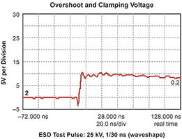
Be sure to look out for disconnects between the electrical characteristics and the information in the plots. Usually, any ‘specification embellishment’ goes on in the plots. For example, Figure 1 shows one vendor’s overshoot and clamping plot, which suggests the result of an ESD test pulse of 25 kV with a 1/30 nanosecond waveshape. However, the waveshape does not directly relate to any standard ESD pulse from either the HBM or IEC standard. It could be used to approximate either standard, but the reader would have to know which one because, between the two, the amount of energy is so different.
The 30 nanosecond point (i.e., the 50% point of the fall time) is also atypical. Typically, this is how a lightning pulse is stated. Therefore, the test pulse being used may not have as much energy as a standard IEC pulse and is not truly comparable on a 1-to-1 basis. Also, the overshoot shown in the plot is practically impossible to achieve. It does not reflect the effects of inductance, due to the 1 nanosecond rise time that would create a spike of at least 30 – 40 V, which is far higher than the 10 V shown in this plot. This leads one to believe a rather slow oscilloscope was used to capture the waveform or that there could be some data ‘post processing’ going on.
In addition to the problems with the waveshape, it’s important to note that this result doesn’t match the electrical characteristics. The minimum breakdown voltage for the device is listed as 6 V, so let’s assume the device turns on at that level. In examining the plot, we see that it clamps to 10 V after a 25 kV strike, which would equate to 93,75 A going through the ESD protector if this were an IEC pulse. Therefore, in order to achieve a 10 V clamp, a 4 V increase over the breakdown, the dynamic resistance would have to be 0,042 Ω. Not only is this value unrealistic, it contradicts the dynamic resistance result we could calculate from the clamping voltages in the electrical specification table (which, in this case, would be closer to 2 Ω). When considered collectively, it’s clear something is amiss, adding further evidence of the need for diligence when reviewing any ESD protection device’s datasheets.
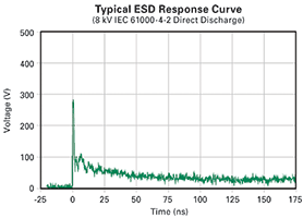
Now, let’s compare the misleading overshoot and clamping voltage plot with a more typical clamped ESD waveform (Figure 2) that shows the characteristic shape. Not only does Figure 2 illustrate the classic waveshape but also the initial peak voltage that’s seen when trying to measure this clamped waveform due to parasitic inductance on the PCB trace. For this reason, judging performance based on plots is seldom the best way to determine the effectiveness of a protection device.
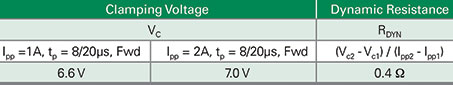
A savvy electronics circuit designer will always use the specification of dynamic resistance to compare ESD protection devices because this removes all secondary effects and indicates how well a device will protect an IC during an ESD over-voltage event or clamp the voltage. Manufacturers like Littelfuse will always provide the dynamic resistance as a separate line item in the datasheet (Figure 3), but it can also easily be calculated by using the clamping voltage at known current levels.
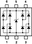
An important point to note about clamping voltage is that some vendors specify it but test only the centre TVS (zener diode) inside a diode array, rather than the combination of steering diode(s) plus zener, which is what one would see looking from a given protected I/O to ground (Figure 4). The device’s clamping voltage spec looks better when disregarding the effects of the steering diode(s), but obscures its actual performance in a circuit.
In contrast, Littelfuse always tests and specifies clamping voltage using a known, repeatable waveshape, such as an 8/20 μs pulse from a given I/O to ground (or I/O to I/O in some cases). In doing so, all circuit elements are included to show the actual clamping performance a designer can expect from the device itself.
The capacitance of an ESD protection device can be measured in many different ways. It is often difficult to compare the performance of different protection devices simply by reading the datasheet. Some vendors test their devices’ capacitance by using a DC bias on the power supply pin (Vcc) and the I/O to show a lower capacitance value. This can be especially misleading if a large DC bias is applied, because the higher the bias used, the lower the capacitance characteristic will be.
Sometimes, the DC bias that is used to measure the capacitance could be much higher than what is actually available in the system or application. To assure greater confidence in the capacitance of a device under consideration, look for a capacitance spec that notes the measurement was taken at 0 V because this is the worst-case capacitance level. In most cases, the value will only get lower when a DC bias is added.
Another ‘trick’ frequently used in datasheets is specifying the capacitance of only one steering diode in order to make the component’s performance look better. The circuit actually sees two steering diodes between the power rails (Figure 4), so the data line would have twice as much capacitance to overcome as the datasheet indicates. In many high-speed applications like USB or HDMI, this could lead to signal integrity issues or outright system failure.
To help designers select the right device for the application, Littelfuse tests and specifies capacitance in no less than three ways for each datasheet. The capacitance is always measured at 0 V bias, measured at a DC bias (usually 2,5 V or 5 V), and illustrated in a plot over a range of DC biases from 0 V to the device’s VRWM or standoff voltage.
Conclusion
In order to prevent potential problems due to insufficient ESD protection in a new electronics design, always remember the following guidelines:
• Keep in mind that some ESD device vendors consider their datasheets part of their marketing effort, so they may be tempted to position their devices as being applicable for uses for which they aren’t particularly well suited.
• Review the datasheet carefully, including all captions and footnotes, and remember that ‘the big print giveth and the small print taketh away.’
• If the electrical characteristics specs seem to be in conflict with the information in the performance plots, be particularly sceptical about the information in the plots, especially if the vendor doesn’t provide information on how the plot was obtained.
Ultimately, distinguishing between a device’s actual performance and marketing hype requires constant diligence. If a spec or plot seems too good to be true, it might very well be misleading.
For more information contact Jeva Narian, Arrow Altech Distribution, +27 (0)11 923 9600, [email protected], www.arrow.altech.co.za
| Tel: | +27 11 923 9600 |
| Email: | [email protected] |
| www: | www.altronarrow.com |
| Articles: | More information and articles about Altron Arrow |


© Technews Publishing (Pty) Ltd | All Rights Reserved
 printer friendly version