


Details of the development of the world's first continuous all-silicon laser on a chip, using standard silicon manufacturing processes, have been disclosed in the 17 Feb edition of the scientific journal, Nature. The scientific breakthrough could help bring low-cost, high-quality lasers and optical devices to mainstream use in computing, communications and medical applications.
Scientists from Intel have used the so-called Raman effect and silicon's crystalline structure, to amplify light as it passes through it. When infused with light from an external source, the experimental chip produces a continuous, high-quality laser beam. While still far from becoming a commercial product, they said that the ability to build a laser from standard silicon could lead to inexpensive optical devices that move terabytes of data inside and between computers at the speed of light - ushering in a flood of new applications for high-speed computing.
Technical details
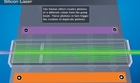
Building a Raman laser in silicon begins with etching a waveguide - a conduit for light on a chip. Silicon is transparent to infrared light so that when light is directed into a waveguide it can be contained and channelled across a chip. Like the first laser developed in 1960, the Intel researchers used an external light source to 'pump' light into their chip. As light is pumped in, the natural atomic vibrations in silicon amplify the light as it passes through the chip. This amplification - the Raman effect - is more than 10 000 times stronger in silicon than in glass fibres. Raman lasers and amplifiers are used today in the telecom industry and rely on kilometres of fibre to amplify light. By using silicon, Intel researchers were able to achieve gain and lasing in a silicon chip just a few centimetres in size.
A laser is widely considered to be any device that emits an intense, coherent beam of light (where the photons all have the same wavelength, phase, and direction). By coating the sides of the chip with a reflective thin-film material, similar to coatings used on high-quality sunglasses, the team was able to contain and amplify the light as it bounced back and forth inside the chip. As they increased the pump energy a critical threshold point was reached, where instantaneously, a very precise beam of coherent light (ie, laser) exited the chip.
Initially, they discovered increasing the light pump power beyond a certain point no longer increased amplification and eventually even decreased it. The reason was a physical process called 'two-photon absorption', which occurs when two photons from the pump beam hit an atom at the same time and knock an electron away. These excess electrons build up over time and collect in the waveguide until they absorb so much light that amplification stops.
Intel's breakthrough solution was to integrate a semiconductor structure, technically called a PIN (P-type - Intrinsic -N-type) device into the waveguide. When a voltage is applied to the PIN, it acts as a vacuum, and removes most of the excess electrons from the light's path. The PIN device combined with the Raman effect produces a continuous laser beam.
For more information and a copy of the paper can be found at www.intel.com/technology/sp.


© Technews Publishing (Pty) Ltd | All Rights Reserved
 printer friendly version