


HP announced that its researchers have created a new way to design future nano-electronic circuits using 'coding theory' - an approach currently being used in certain math, cryptography and telecom applications.
The result could be nearly perfect manufacturing yields with equipment a thousand times less expensive than what might be required using future versions of current technologies.
In the 6 June issue of the Institute of Physics' 'Nanotechnology' magazine, authors Phil Kuekes, Warren Robinett, Gadiel Seroussi and Stan Williams of HP Labs explain in detail a defect-tolerant interface to HP's patented crossbar architecture.
"We have invented a completely new way of designing an electronic interconnect for nano-scale circuits using coding theory, which is commonly used in today's digital cellphone systems and in deep-space probes," said Williams. "By using a cross-bar architecture and adding 50% more wires as an 'insurance policy', we believe it will be possible to fabricate nano-electronic circuits with nearly perfect yields even though the probability of broken components will be high."
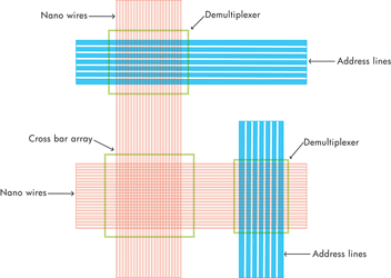
Williams said he believes future chips will have to rely, at least in part, on the crossbar architecture, in which a set of parallel nanoscale wires are laid atop another set of parallel wires at approximately a 90° angle, sandwiching a layer of electrically switchable material in between. Where the material becomes trapped between the crossing wires, they can form a switch that represents a '1' or '0', the basic building blocks of computer code.
Future chips may be limited in the geometric complexity that can be created at the nano level because of problems with precision alignment. Crossbar structures are highly regular and therefore relatively easier and less expensive to fabricate than the complex array of wires, transistors and other elements in today's processors. The disadvantage of crossbars is that they require more space on the silicon.
"We think the tradeoff of space versus manufacturing ease will become more an issue in the near future," said Williams. "Furthermore, as sizes of electronic features get down to a few nanometers, it will become either physically impossible - or economically unfeasible - to produce absolutely perfect circuits."
In HP's approach, a demultiplexer enables data to be read and written in a circuit by connecting the crossbar array of nanowires to a small number of conventional wires. By adding a few more conventional wires and using basic coding theory, the researchers show that the demultiplexer still works even if a significant number of the connections between the conventional wires and the nanowires are broken.
"It is like giving a distinctive name to a restaurant host to be sure you hear your party called above the noise of the crowd," said senior computer architect Kuekes. "Instead of 'the Jones party', you might put yourself down as 'the John Paul Jones party'. That way, when the host calls your name, you will hear it, even if every word does not come through clearly."
Using defect tolerance to replace the need to produce 'perfect' chips could provide a huge cost advantage for chip manufacturers in the future.
Williams said the HP Labs group has created working devices in the laboratory at the 30 nanometer half-pitch scale - about a third the size of today's chips. The International Technology Roadmap for Silicon, the standard for the industry, predicts that chips using features at 32 nanometers half pitch should be in production in about seven to eight years.






© Technews Publishing (Pty) Ltd | All Rights Reserved
 printer friendly version