The key is ... nothing
13 June 2007
News
Information from Frost & Sullivan Technical Insights
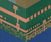
By making use of an innovative technique, researchers at IBM have been able to surround copper wires within electronic chips with an insulating vacuum - an advance that should lead to more efficient processors. The patented approach, which the researchers call 'airgap', is currently integrated into one IBM production facility. The company says that the technology should be in use in all its production lines by 2009, and will be integrated into chips at the 32 nm node.
Rather than using a photolithographic approach to create the structures, the IBM team made use of self-assembly, a technique being eagerly explored by nanotechnology researchers. In the technique, chemical or structural properties found in molecules or structures are used to encourage the materials to order themselves into patterns.
Empty space between the microprocessor’s wiring
"This is the first time anyone has proven the ability to synthesise mass quantities of these self-assembled polymers and integrate them into an existing manufacturing process with great yield results," said Dan Edelstein, one of the researchers on the project. A mix of polymers is poured onto a chip and then baked, yielding a pattern of tiny holes. The glass coating on the wires is etched away, and another layer of glass is applied over the top of the hole-riddled polymer in a vacuum chamber, sealing off the holes, and leaving vacuum-filled chambers inside.
Normally, the tiny wires in a microchip are separated by an insulating material to prevent interference between wires. However, as chip feature sizes continue to scale downwards, finding high-quality insulating layers with the right electronic properties is becoming more difficult, and current leakage due to capacitance issues - which in turn leads to unwanted heat - is becoming more of a problem. Replacing the insulating material with a vacuum, Edelstein said, allows for better performance than would be possible with equally sized amounts of conventional materials. He estimated that using the approach, it should be possible to boost chip speeds by 35% compared to conventional methods, or to reduce power consumption by 15%.
For more information contact Frost & Sullivan Technical Insights, +27 (0)21 680 3274, [email protected]
Further reading:
From the editor's desk: The art of measuring the truth
Technews Publishing
Editor's Choice News
All electronic measurements are a lie. The trick is making the lie as small as possible.
Read more...
TSE has relocated
News
The Technology Station in Electronics (TSE) has entered a new chapter with its relocation from the CSIR campus to TUT-owned building at Ditsela Place in Hatfield.
Read more...
Innovative MyLegrand app
RS South Africa
News
Legrand SA is set to launch the MyLegrand mobile application, a digital platform designed to strengthen engagement across its professional network.
Read more...
Kulani Energy acquires critical assets from Optipower
News
Kulani Energy preserves engineering, procurement, and construction capability and positions a wholly women-owned firm at the forefront of South Africa’s grid expansion.
Read more...
From Cape Town to Johannesburg
News
Würth Elektronik South Africa has taken a significant step forward with its recent relocation from Cape Town to Johannesburg, marking a new phase of growth and ambition for the company.
Read more...
Lesley Havenga: Building partnerships for Africa’s electronics future
Editor's Choice News
As Würth Electronik expands its footprint across South Africa and the broader sub-Saharan region, Havenga’s blend of manufacturing expertise, supply chain knowledge, and people-centred leadership appears well suited to the task.
Read more...
Tackling e-waste with help from international partners
News
Every year millions of electrical and electronic devices and appliances, including mobile phones and computers, are thrown away and these items are now the fastest growing waste stream in the world.
Read more...
From the editor's desk: Pricing surge reshapes engineering reality
Technews Publishing
News
The recent and continuing surge in memory prices has become more than a supply-chain story confined to global semiconductor markets. We have watched in disbelief as the ASP of memory has risen by over
...
Read more...
Siemens democratises EDA software access
News
This collaboration will provide streamlined access to advanced electronic design automation software for European semiconductor innovation.
Read more...
Components distribution: A promising trend
News
The European electronic components market returned to solid growth in Q1, gaining 16,9%, with broad, but uneven, momentum across the region.
Read more...


 printer friendly version