23 April 2003Manufacturing / Production Technology, Hardware & Services
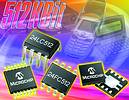
Microchip says that its new 512 Kb I2C compatible serial EEPROMs are the first to be available in an 8-pad dual flat no-lead package. The 6 x 5 x 0,9 mm DFN packages are ideal for low-headroom applications, reducing cost and increasing available board space.
The 24LC512, 24AA512, and 24FC512 devices use Microchip's advanced PMOS electrically erasable cell process technology to produce high-density, low-power EEPROMs in one of the thinnest packages available. PEEC process technology also ensures reliability, achieving more than 200 years data retention and 1 000 000 erase/write cycles at 85°C. Users of its 128 Kb or 256 Kb EEPROMs can use these higher-density EEPROMs while retaining the same footprint, says the company. Additional packages include an 8-lead PDIP, 8-lead SOIC and 14-pin TSSOP.
The devices have a page-write capability of up to 128 bytes and can perform random reads throughout the entire array. Functional address lines allow up to eight devices on the same bus for a maximum of 4 Mb total address space. Additional features include a fast write time of 5 ms, a clock rate of 400 kHz throughout the operating voltage of 2,5 V-5,5 V and temperature range of -40 to +85°C. The 24FC512 can operate at a bus speed of 1 MHz and the 24 AA512 has an operating voltage of 1,8 V-5,5 V.
For more information contact Avnet Kopp, 011 809 6100, Memec SA, 021 674 4103, Tempe Technologies, 011 452 0530.
FineX: Makes shielding clear Avnet Abacus
Manufacturing / Production Technology, Hardware & Services
Panasonic Industry launches high-transparency, low-resistance, flexible transparent conductive film for electromagnetic wave shield with pre-applied OCA.
Read more...Collaboration is now critical RS South Africa
Manufacturing / Production Technology, Hardware & Services
The message emerging from RS Connect is clear: Organisations can no longer rely on internal optimisation alone to secure performance. Competitive advantage is increasingly being determined by the strength of external relationships, shared capability and coordinated action across value chains.
Read more...Disruption is the new normal. Effortless is the new competitive advantage. Seven Labs Technology
Manufacturing / Production Technology, Hardware & Services
Global supply chains have been under pressure for years. The manufacturers still standing are the ones who stopped waiting for normal to return, and started building something better.
Read more...World-first 016008 mm component placement
Manufacturing / Production Technology, Hardware & Services
Fuji has achieved the world’s first placement of 016008 mm (0,16 x 0,08 mm or 006 x 003 inches) size components on printed circuit boards with its SMT pick and place machine, NXTR.
Read more...Lifecycle and obsolescence: Protecting electronics through process Production Logix
Manufacturing / Production Technology, Hardware & Services
At Production Logix, we believe longevity is not accidental. It is engineered through early visibility, structured response, and disciplined execution, in partnership with our OEM customers.
Read more...Maximising squeegee quality and durability Testerion
Manufacturing / Production Technology, Hardware & Services
Transition Automation has announced two new product advancements designed to improve SMT printing performance and extend squeegee life: laser-enhanced Permalex bonding and integrated edge protectors.
Read more...NeoDen ND2 PCB screen printer ZETECH ONE
Manufacturing / Production Technology, Hardware & Services
The NeoDen ND2 PCB screen printing machine is a fully automatic stencil printer designed to deliver precise and consistent solder paste application in modern SMT production environments.
Read more...Understanding the BGA rework process Techmet
Manufacturing / Production Technology, Hardware & Services
BGA rework is a highly technical process that involves removing the faulty component, preparing the circuit board, and installing a new or repaired device, while maintaining the integrity of the printed circuit board.
Read more...Flexible three-process reflow soldering system Truth Electronic Manufacturing
Manufacturing / Production Technology, Hardware & Services
By combining multiple soldering technologies within a single system, the Vision TripleX system enables manufacturers to adapt easily to different assembly requirements, board designs, and production volumes.
Read more...Inline vapour phase soldering for high-volume production MyKay Tronics
Manufacturing / Production Technology, Hardware & Services
The VP2200-100 vacuum inline vapour phase soldering system from ASSCON is designed for fully automated, high-volume electronics manufacturing where process consistency and solder joint quality are critical.
While every effort has been made to ensure the accuracy of the information contained herein, the publisher and its agents cannot be held responsible for any errors contained, or any loss incurred as a result. Articles published do not necessarily reflect the views of the publishers. The editor reserves the right to alter or cut copy. Articles submitted are deemed to have been cleared for publication. Advertisements and company contact details are published as provided by the advertiser. Technews Publishing (Pty) Ltd cannot be held responsible for the accuracy or veracity of supplied material.


 printer friendly version