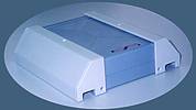
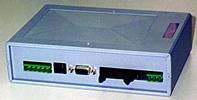
The K-Box process - an innovative concept in enclosure technology
25 October 2000
Manufacturing / Production Technology, Hardware & Services
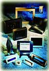
A few years ago the idea of having a custom made plastic enclosure for your electronics and keeping the costs for prototyping and limited production runs below R10 000 seemed ludicrous. However, with the introduction of the PMP process, developed and perfected by TTK Kunststoff of Germany, this is no longer a fantasy.
K-Box Technology SA, the South African licence holder for the process, is offering this innovative method of enclosure manufacture to the local market. As most designers will know, gaining a 'competitive edge' could be something as small as the 'look and feel' of the packaging and having the ability to really make one's product stand out in the crowd can be a huge plus point. The fact that K-Box manages to manufacture these enclosures without the need for tooling or moulds and that the designs can be changed at any point during the life of the product makes a telling point against investing thousands of rands in injection moulding processes.
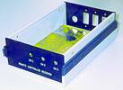
The PMP process involves the fabrication of enclosures using milled flat panels that are then bent and assembled to the same strict tolerances required of injection-moulded products. Using the specially designed software and NC milling machines K-Box is able to design and manufacture a prototype housing in as little as one week or, if the need requires, even overnight.
That is one of the major advantages of the process. With the life expectancy of most electronics now being measured in months rather than years, the ability to repackage electronics if and when needed has become critical. Be it because of technology updates or styling, K-Box is in the position to design a box around one's electronics that can be modified at will.
K-Box has housed electronics in a variety of applications including: access control, time and attendance, medical, industrial control, forecourt POS, thin clients, promotional and marketing, and many others
Further reading:
FineX: Makes shielding clear
Avnet Abacus
Manufacturing / Production Technology, Hardware & Services
Panasonic Industry launches high-transparency, low-resistance, flexible transparent conductive film for electromagnetic wave shield with pre-applied OCA.
Read more...
Collaboration is now critical
RS South Africa
Manufacturing / Production Technology, Hardware & Services
The message emerging from RS Connect is clear: Organisations can no longer rely on internal optimisation alone to secure performance. Competitive advantage is increasingly being determined by the strength of external relationships, shared capability and coordinated action across value chains.
Read more...
Disruption is the new normal. Effortless is the new competitive advantage.
Seven Labs Technology
Manufacturing / Production Technology, Hardware & Services
Global supply chains have been under pressure for years. The manufacturers still standing are the ones who stopped waiting for normal to return, and started building something better.
Read more...
World-first 016008 mm component placement
Manufacturing / Production Technology, Hardware & Services
Fuji has achieved the world’s first placement of 016008 mm (0,16 x 0,08 mm or 006 x 003 inches) size components on printed circuit boards with its SMT pick and place machine, NXTR.
Read more...
Lifecycle and obsolescence: Protecting electronics through process
Production Logix
Manufacturing / Production Technology, Hardware & Services
At Production Logix, we believe longevity is not accidental. It is engineered through early visibility, structured response, and disciplined execution, in partnership with our OEM customers.
Read more...
Maximising squeegee quality and durability
Testerion
Manufacturing / Production Technology, Hardware & Services
Transition Automation has announced two new product advancements designed to improve SMT printing performance and extend squeegee life: laser-enhanced Permalex bonding and integrated edge protectors.
Read more...
NeoDen ND2 PCB screen printer
ZETECH ONE
Manufacturing / Production Technology, Hardware & Services
The NeoDen ND2 PCB screen printing machine is a fully automatic stencil printer designed to deliver precise and consistent solder paste application in modern SMT production environments.
Read more...
Understanding the BGA rework process
Techmet
Manufacturing / Production Technology, Hardware & Services
BGA rework is a highly technical process that involves removing the faulty component, preparing the circuit board, and installing a new or repaired device, while maintaining the integrity of the printed circuit board.
Read more...
Flexible three-process reflow soldering system
Truth Electronic Manufacturing
Manufacturing / Production Technology, Hardware & Services
By combining multiple soldering technologies within a single system, the Vision TripleX system enables manufacturers to adapt easily to different assembly requirements, board designs, and production volumes.
Read more...
Inline vapour phase soldering for high-volume production
MyKay Tronics
Manufacturing / Production Technology, Hardware & Services
The VP2200-100 vacuum inline vapour phase soldering system from ASSCON is designed for fully automated, high-volume electronics manufacturing where process consistency and solder joint quality are critical.
Read more...


 printer friendly version