


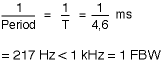
Many devices, including the GSM power amplifiers used in cellular handsets, were not designed to operate continuously. The GSM system operates in the 900 or 1800 MHz bands and uses Gaussian minimum shift keying (GMSK), which is a type of digital FM modulation. The output power is measured during a burst, which is 577 µs long and repeats every 4,6 ms. Traditional measurement techniques are not adequate for this type of burst signal.
Therefore, pulsed-RF techniques must be employed during this burst period for accurate measurements of s-parameters.
This article provides an application guide to understanding general s-parameter measurements with a vector network analyser under pulsed-RF conditions for GSM power amplifiers. Most modern vector network analysers have a receiver and trigger functionality to make such measurements. A brief description of pulsed-RF measurements, the test set-up for a GSM amplifier and some s-parameter results are presented.
Pulsed RF signals
Most power amplifiers (PAs) are not designed to transmit with 100% duty cycle. If they were, the PA device would heat up, drawing considerable current. Transistors tested on a wafer would be subject to extreme heating, causing thermal stress. To avoid this problem, s-parameter measurements are often taken with the PA in a pulsed condition.
A pulsed RF signal (PRF) will have a frequency spectrum composed of a series of spectral lines with an envelope described by a sinc function (ie, sin(x)/x). The spacing of the lines ("1/T") is set by the PRF frequency while the envelope shape is fixed by the pulse width (assuming small rise and fall times to pulse width). The spacing of the spectral lines is equal to 1/period = 1/T as shown in Figure 1.
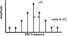
The GSM signal is a 577 µs pulse with a period of 4,6 ms, which equates to a PRF frequency of approximately 217 Hz. This spectrum's 'size' determines how much IF bandwidth (IFBW) is necessary in the vector network analyser (VNA) receiver for accurate PRF measurements. In this case, the entire spectrum can fit within an IFBW of 1 kHz:
There may be some outlying spectral components at the edges so some additional averaging may be needed to reduce the effects of the edge frequency components. The VNA must be aligned in time with the PRF; otherwise, all the transmitted s-parameter data points will not be collected properly. This is the fundamental reason for an externally 'triggered' signal to the VNA.
Triggered measurements
As shown by Equation 1, the received signal captured by the VNA fits entirely inside a typical IFBW (ie, 1 kHz), which can be set between 1 and 30 kHz in most VNAs. In the time domain, the sampling needs to occur during the amplifiers' 'on-period' of the pulse in order to capture the s-parameter data. This is achieved by externally triggering the VNA to measure the appropriate points in time. As shown in Figure 2, the external trigger pulse arrives at the VNA some time before the RF pulse in order to account for the 'latency' inside the VNA. 'Latency' is the term used to describe the delay from one transmission point to another. Latency occurs in many electronic systems where there is a propagation delay between source and receiver.
In this case, the VNA requires a delay between its received external trigger signal and the Tx-Enable signal. According to an Anritsu application note, the delay should be on the order of 50 to 100 µs although starting later is allowed. The sampling can begin sometime after the RF pulse has settled unless the initial data points are of additional interest. The sampling can continue for a substantial portion of the pulse but should not continue beyond the end of the pulse.
As a general rule, the IFBW must be greater than 1/pulse width to keep sampling from overrunning the pulse (IFBW = 10 kHz with averaging turned on is acceptable on the Anritsu MS4623B VNA). Due to pulse settling time, VNA internal filtering and latency issues, some safety margin is required. This will vary greatly depending on set-up and may require some experimentation. If the IFBW is too small, the sampled s-parameters will contain some noise as a result of not completely capturing the full GSM burst.
Measurement set-up
In order to validate the theory, the RF Micro Devices RF3110 quad-band power amplifier will be measured and S11 and S21 s-parameters captured on the Agilent MS4623B vector network analyser (VNA) using an Anritsu Display Capture program.
The test set-up is shown in Figure 3. It includes an arbitrary waveform generator (AWG 320) for the ramp profile and a 2,5 Vp-p square wave trigger signal, which was used to synchronise the VNA with the Transmit Enable (Tx-En) signal on the RF3110 (see Figure 4).
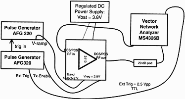
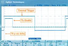
In order to achieve a 'leading' external trigger signal, the phase angle of the trigger signal was then changed to allow offset waveforms. The trigger signal should lead the Tx-Enable signal by 50 to 100 µs. A lead time of 70 µs corresponds to a phase setting of 32 degrees on the AFG 320 arbitrary waveform generator.
A calibrated input signal of -10 dBm was applied to the input port of the RF3110 evaluation board (EVB). A 20 dB attenuator was also placed at the output port to avoid saturating the VNA front end, which accepts a received signal of +5 dBm. DC voltages were also sequentially applied to Vreg (2,8 V) and Band-Select (2 V). A Vramp waveform of 1,4 V that conforms to the ETSI timing mask was then applied to the RF3110 in order to take the full-power s-parameter measurements.
S-parameter measurements
Small-signal measurements of S21 and S11 were taken on the RF3110. Associated plots are shown in Figures 5, 6 and 7. S21 represents the actual gain of the device and S11 reveals the input impedance when the device is turning off and on. Without using triggered measurements both of these parameters would not be accurately reported. S22 data is not collected since it represents the output impedance of the RF3110, which is meaningless for impedance matching to the antenna.
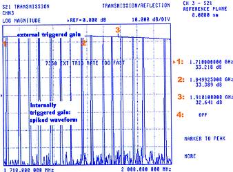
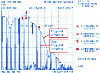
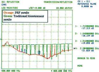
Figure 5 shows the gain plot for the external and internal triggered measurement. The top line is the gain curve for the VNA externally triggered and its markers are shown to the right (ie, 32 dB of gain). The default internally triggered signal shows spikes, indicating that the VNA is not capturing the gain (S21) of the transmitted GSM signal correctly. The 'external trigger rate too fast' message is superficial and only occurs with the VNA screen capture operation.
Figure 6 shows the same plot over larger frequency band.
The effects of externally triggering the GSM amplifier for the input reflection coefficient, S11, is shown in Figure 7.
Conclusion
A technique for pulsed S-parameter measurements on GSM amplifiers has been presented along with some details on how to make successful measurements using a network analyser. Plots of S11 and S21 for a pulsed RF signal with an external and internal trigger are displayed to show the results of using the external trigger on the VNA for PRF environments. It is the hope of the author that this information may be beneficial to those taking small-signal measurements on devices with pulsed RF.
| Tel: | +27 21 555 8400 |
| Email: | [email protected] |
| www: | www.rfdesign.co.za |
| Articles: | More information and articles about RF Design |


© Technews Publishing (Pty) Ltd | All Rights Reserved
 printer friendly version