


Power amplifiers used in basestations require biasing for proper RF performance. This article explains the two classes of biasing that are prevalent in the RF industry, analyses their characteristics, and shows implementations with existing ICs.
The power device of choice for basestation amplifiers today is the lateral DMOS (LDMOS) MOSFET, and is used in this article to illustrate biasing techniques. However, as future generations of devices become available, such as GaN FETs, HFETs, or SiC devices, they too will benefit from the following implementations.
RF classes and biasing
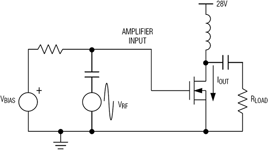
LDMOS amplifiers used in RF circuits exhibit varying degrees of nonlinearity, depending on the DC-bias level upon which the input RF waveshape rides. That is, while maintaining a constant RF gating signal, the output current's (Iout) harmonic content varies as the DC bias at the gate of an LDMOS device (Figure 1) changes. The harmonic content of the LDMOS amplifier's current is important because, in the RF load, it creates power interference with the local bandwidth (in-band interference) or with adjacent bandwidths (out-of-band interference).
The best linearity occurs when the output current tracks the input voltage - a 360° conduction angle. Operating the MOSFET in this manner (ie, class-A operation) creates less distortion than when biasing it in any other way. From a power-dissipation perspective, however, class-A operation is least desirable because it consumes the most DC current.
At high RF power, given a nominal power-supply voltage of 28 V, the DC power dissipated in the amplifier is prohibitive. For this reason, RF engineers use class-AB biasing in the last stage of an amplifier chain, while they favour class-A operation in the preceding stages where power dissipation is smaller by orders of magnitude. In class-AB stages, the output current does not track the input voltage entirely, and thus the amplifier's conduction angle is lower than 360°.
Distortion of the RF signal in class AB is more significant than in class A. The spectrum of this distortion is wider and more densely populated than that of class A. However class-AB power dissipation is lower because the average current into the amplifier is lower. In short, the basis for choosing a given class of commercial RF amplifiers is a tradeoff between linearity and efficiency.
Biasing requirements and LDMOS behaviour
Biasing requires managing the DC content in the LDMOS current across temperature and supply variation. The ultimate objective is to ensure that the amplifier RF gain, as well as its distortion levels, varies within limits consistent with requirements. In this respect, proper biasing can assist linearisation techniques to minimise distortion.
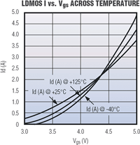
The equation governing LDMOS's gain is Iout = K (Vgs - Vth)², where K is a constant reflecting gain due to electron mobility and Vth is the FET's threshold. Both K and Vth are temperature dependent. In Figure 2, LDMOS characteristics are shown across temperature. In class AB, designers tend to operate the bias to the left of the crossover region where the gain has a positive temperature coefficient. In class A, operation occurs to the right of the crossover region.
Controlling A and AB bias with the DS1847
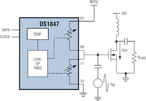
Figure 3 shows a DS1847 dual, temperature-controlled variable resistor controlling the gate of an LDMOS amplifier. The DS1847's internal temperature sensor provides a temperature reading to its look-up tables. These look-up tables adjust the IC's two 256-position variable resistors so the amplifier's gate receives the proper bias voltage. The user programs the look-up tables to generate a constant LDMOS-amplifier output current. Refer to Figure 2 (or to manufacturer-specific data curves) for LDMOS characteristics. By using the two resistors to attenuate the reference voltage, a temperature-insensitive voltage is maintained.
| Tel: | +27 11 608 0070 |
| Email: | [email protected] |
| www: | www.cstelectronics.co.za |
| Articles: | More information and articles about CST Electronics |


© Technews Publishing (Pty) Ltd | All Rights Reserved
 printer friendly version