


The capture, compare and PWM (CCP) modules that are found on many of Microchip Technologies' microcontrollers are used primarily for the measurement and control of time-based pulse signals. The enhanced CCP (ECCP), available on some of the company's devices, differs from the regular CCP module in that it provides enhanced PWM functionality - namely, full-bridge and half-bridge support, programmable dead-band delay and enhanced PWM auto-shutdown. The ECCP and CCP modules are capable of performing a wide variety of tasks.
In this article Microchip offers a few 'tips and tricks' that describe some of the basic guidelines to follow when using these modules, as well as suggestions for practical applications.
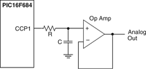
Tip 1 - Generating an analog output
Pulse-width modulated (PWM) signals can be used to create digital-to-analog (D/A) converters with only a few external components. Conversion of PWM waveforms to analog signals involves the use of an analog low-pass filter. In order to eliminate unwanted harmonics caused by a PWM signal to the greatest degree possible, the frequency of the PWM signal (FPWM) should be significantly higher than the bandwidth (FBW) of the desired analog signal. Equation 1a shows this relation.
Equation 1a: FPWM = K*FBW
Where harmonics decrease as K increases
R and C are chosen based on the following equation:
Equation 1b: RC = 1/(2π FSW)
Pick a value of C arbitrarily and then calculate R. The attenuation of the PWM frequency for a given RC filter is:
Equation 1c: Att(dB) = -10*log[1+ (2π FPWM R C)2]
If the attenuation calculated in Equation 1c is not sufficient, then K, in Equation 1a, must be increased.
For more details on using PWM to generate an analog output see Application Note AN538 on Microchip's website.
Tip 2 - Boost power supply
Pulse-width modulation (PWM) plays a key role in boost power supply design. Figure 2 shows a typical boost circuit. The circuit works by Q1 grounding the inductor (L1) during the high phase of the PWM signal generated by CCP1. This causes an increasing current to flow through L1 while VCC is applied. During the low phase of the PWM signal, the energy stored in L1 flows through D1 to the storage capacitor (C2) and the load. VOUT is related to VIN by Equation 2a.
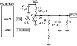
The first parameter to determine is the duty cycle (D) based upon the input and output voltages. See Equation 2a.
Equation 2a: VOUT/VIN = 1/(1 - D)
Next, the value of the inductor is chosen based on the maximum current required by the load, the switching frequency and the duty cycle. A function for inductance in terms of load current is given by Equation 2b, where T is the PWM period, D is the duty cycle and IOUT is the maximum load current.
Equation 2b: L = [VIN (1 - D) D T]/[2 IOUT]
The value for L is chosen arbitrarily to satisfy this equation given IOUT, a maximum duty cycle of 75% and a PWM frequency in the 10 kHz to 100 kHz range.
Using the value chosen for L, the ripple current is calculated using Equation 2c.
Equation 2c: IRIPPLE = VIN D T/L
IRIPPLE cannot exceed the saturation current for the inductor. If the value for L does produce a ripple current greater than ISAT, a bigger inductor is needed. Note: All equations above assume a discontinuous current mode.
Firmware
The PWM duty cycle is varied by the microcontroller in order to maintain a stable output voltage over fluctuating load conditions. A firmware-implemented PID control loop is used to regulate the duty cycle. Feedback from the boost power supply circuit provides the input to the PID control.
Details on boost power supply design are provided in Technical Brief TB053, while Application Note AN258 provides details on firmware-based PID control. They can be found on Microchip's website.
Tip 3 - Generating X-10 carrier frequency
X-10 is a technology developed to communicate between transmitters and receivers by sending and receiving signals over the power line wiring. These signals involve short RF bursts which represent digital information (see www.x10.com/support/technology1.htm).
The X-10 protocol uses a piggybacked 120 kHz square wave (at 50% duty cycle) to transmit information over 60 Hz power lines. The CCP module, running in PWM mode, can accurately create the 120 kHz square wave, referred to as the carrier frequency. Figure 3 shows how the 120 kHz carrier frequency is piggybacked onto a sinusoidal 60 Hz power waveform.
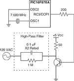
X-10 specifies the carrier frequency at 120 kHz (±2 kHz). The system oscillator in Figure 3 is chosen to be 7,680 MHz, so that the CCP module can generate precisely 120 kHz. X-10 requires that the carrier frequency be turned on and off at different points on the 60 Hz power waveform. This is accomplished by configuring the TRIS register for the CCP1 pin as either an input (carrier frequency off) or an output (carrier frequency on.)
Refer to Application Note AN236 on Microchip's website for more details on X-10 and for source code for setting up the CCP module appropriately.
| Tel: | +27 11 923 9600 |
| Email: | [email protected] |
| www: | www.altronarrow.com |
| Articles: | More information and articles about Altron Arrow |
| Email: | [email protected] |
| www: | |
| Articles: | More information and articles about Tempe Technologies |


© Technews Publishing (Pty) Ltd | All Rights Reserved
 printer friendly version