


Ref: z2816202m
The process of passing FCC/CISPR tests must be approached like open heart surgery. While the part of the procedure that gets a lot of press is the skill of the surgeon who physically replaces the heart valve, arteries, etc, there are many procedures that lead up to that one central dramatic event, and there are many more that follow it in order to achieve a high probability of success.
The main reason customers want to pass FCC tests is so they can ship their product. Normally, the focus is on a dramatic central event like signal integrity analysis but while signal integrity analysis is critically important, it is not sufficient in and of itself. Other events like proper power delivery design, return current control, and crosstalk analysis are critical to give a high probability of success. Ignoring one of these steps can derail the quest for first time success just as much as a septic instrument can jeopardise an otherwise perfect surgical procedure. The operation is successful, but the patient dies of post surgical infection.
This article will outline a methodology developed as a road map for how to pass the critical FCC/CISPR test the first time. Repeatable success in this arena demands a set series of design tasks be executed in an appropriate manner. The methodology described in this paper simply outlines the minimum mandatory steps necessary to achieve first time success.
If you perfect the necessary methods, your:
* Engineering cycle will be much more predictable.
* Products will be much more reliable.
* Overall design time, plus the time into manufacturing, will decrease dramatically.
* Problems like 'hardware software wars' will be greatly diminished because the hardware will be stable and software developers will not waste time trying to invent test code which can distinguish between a software problem and a hardware problem.
If you do not, your:
* Product will probably fail FCC/CISPR tests. And if the product fails, you can not ship it, you do not get paid, and life gets ugly.
If you squeak by the FCC/CISPR tests and you can ship the product, it will probably be tough to manufacture because of inadequate manufacturing design margins. In addition you will probably have warranty return rate problems which affect both the bottom line and also your company's reputation for producing quality products. Again life gets ugly. It just gets ugly slower.
Many times these problems take a significant amount of time to solve. This results in late market entry with the adjunct loss of revenue. Equally important, though, is the strategic loss of engineering resources because the design team is trying to get an old design stable rather than inventing the next killer product which can put the company over the top. I call this engineering opportunity cost.
The same expensive, highly educated people could be designing your follow-on product rather than wasting time fixing something that should have shipped six months ago.
Key elements of a successful HSSD methodology
Correct problems at the source
The primary frame of reference for this discussion is a digital CMOS product with rise times in the <2 ns range, housed in a plastic box with long leads attached. Most of the time I am called into an account because the project is six months late and it has failed at least three trips to the field testing site. The wizards of the EMI labs have already worked their magic long before I arrive on the scene. Hence, I have a perfect batting average. Every time I show up I must tell the customer that they must re-layout their PCB in order to solve their problem. My entire focus is to do it right the first time using rational design methods that produce repeatable results. The design team must fix the problems at their source. If they do, the system will work in a predictable, stable manner...by design.
The alternative method is to think happy thoughts, do your best, and hope the system will pass. Since engineers always believe their designs will work, this method is fun, but not very reliable.
Grasp the holistic nature of the problem
Everything affects everything. For example: ringing causes radiated EMI, false data, false clocking, and reliability problems. If you fix ringing you will also drastically improve radiated EMI, clock and data integrity, and product reliability.
Poor power delivery system performance results in ground (or VCC) bounce. This affects everything including common-mode EMI.
Having a disciplined operating room sanitation type approach
Attention to detail is critical. Again, this methodology is like performing successful open heart surgery. If you have the best surgeon and the best hospital, but fail to sterilise the instruments, the patient can still die of infection. This is not an inherently difficult process, but it is very unforgiving of those who ignore critical details.
Designers must have published gating procedures that the project must pass through before it can move on to the next stage of development.
Be able to predict the effect of layout decisions on the behaviour of the finished design
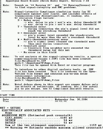
If just one critical trace is not terminated correctly, it can result in false clocking/false data, and radiated EMI issues, as well as manufacturing yield and warranty return problems. If the need for termination is discovered after the board is built, there is no place to put the termination elements. The designer is forced to re-layout and re-prototype the board before any forward progress toward getting the product into production can be made. It is critical to understand the effects of the decisions before they are actually built in the board. This means there must be some method of 'predicting' behaviour. My tool of choice is a simulator because it is quick, accurate, and I can not only get a good/bad answer, but I can also get insight into the sensitivity of the design to various changes I might need to make later in the process. The sensitivity analysis gives me a good indication about where the edge of the cliff is if someone is trying to force me in that direction.
If a designer does not have a simulator suitable for predicting ringing, crosstalk and radiated EMI, their only other choice is to build a test board. When that is done, be sure to build an array of configurations. This will give the designer an appreciation for the sensitivity of the design to various changes that may need to be made.
I am not advocating building the complete design, but I am advocating implementing representative high speed signal paths like the clock and any high speed busses. In the case of a buss, designers do not need all 32 bits, probably four will do nicely. If you build a test board, you need to bracket the length for ringing/EMI, the spacing for cross talk, and include pads for terminations if they are needed.
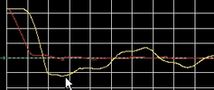

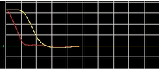
The second set of screen shots below shows the result of proper termination on the circuit and its subsequent performance.
Have check points along the way to verify that you are on track.
Layout designers must know the physical details necessary in order to have a successful implementation. The circuit designer is the only one who has the intimate knowledge about the timing of the circuit. The circuit designer must be able to pass on to the layout designer the physical layout constraints necessary to achieve the electrical performance necessary for proper function. In the layout process, there are constantly small tradeoff decisions. The circuit designer must create a document that contains all of the critical information and this document must be given to the layout designer so the layout designer knows the sensitivity of each critical signal on the board. A major check point is the fact that this analysis is done and recorded properly so the information can be shared with the others on the design team.
A final critical check point would be to run a ringing crosstalk and EMI check against the entire board after it is laid out, but prior to fabrication. If a reasonable process is used, this will not delay the release to production, but it will certainly catch common problems that can cause the board to fail regulator tests.
Correct the process if you do not get the predicted results
The process must be closed loop. The results of the process must be predicted and the final results checked against the predicted result. If the loop is not closed and the process made self-correcting, there is no process.
For example, when a major Canadian telecom company began measuring their process, they found that 94% of the time they needed to re-layout the board due to high speed issues. When they implemented a process which included appropriate analysis and gating functions, they reduced the redesign rate to less than 1%.
Basic concept and terms
Return current
Return current is the part of the circuit that is not on the schematic and is not routed. It is the non-obvious part of the circuit that is just as critical for high speed performance as is the routed signal path. Ignoring the return current path probably results in ringing, crosstalk, and radiated emissions. Any one of these problems can and generally does cause the product to fail.
Controlled impedance/controlled impedance layer pair
Controlled impedance signal traces maintain fixed geometries and known return current paths such that the entire signal routing path displays the desired characteristic impedance. This means designers must not only route the signal trace using rational rules, but they must also add features or components that allow them to see by inspection where the return current flows. It is the summation of the signal current and return current that determines the impedance of the path. Improper signal path impedance can result in a host of errors including radiated EMI.
Ground bounce/SSOn
Ground bounce and simultaneous switched output noise (SSOn) are the result of a poorly-designed power deliver system. In essence the power rails, as seen by the receive comparator, move. This movement or 'ground bounce' makes it more difficult, if not impossible, for the receiver to accurately interpret the signal as a 1 or 0. It is critical to provide a power delivery system that holds the ground bounce/SSOn to some arbitrarily low value like 100 mV or less from DC to the highest frequency of interest. For a sub 2 ns rise time signal, the highest frequency of interest is over 1 GHz.
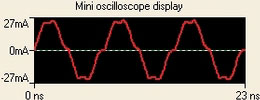
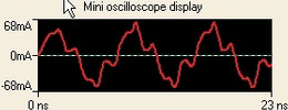
There are four key elements for predicting ground bounce. First, designers need to know the peak current delivered by a single output driver. This is layout dependent. Ringing can more than double the current draw on a driver resulting in false clocking, false data, and nasty reliability problems. Proper termination will drastically lower driver currents and present a far easier task for the power deliver system to control ground (and VCC) bounce.
Second, designers need to know how many of these drivers are firing at the same time. Delivering 30 mA is not bad, but if 32 of them fire at the same time that is nearly an Amp. Often that 960 mA pulse of current must be delivered in sub-nanosecond time.
Third, we need to know the power plane impedance. This is the aggregate impedance of the power supply plus the contribution due to all of the capacitors on the board. If these are connected in the wrong manner, they rapidly become useless as frequency increases.
Finally, designers need to know how much current is supplied by a single power delivery via. The inductance of the via results in a significant voltage drop at higher frequencies. Assuming designers have these numbers and connect everything in a consistent manner, they can predict ground bounce and SSOn.

Ringing
Ringing is an electrical echo that distorts the clock or data signal. This results in false clocks, false data and hardware reliability problems. Ringing is also the most common cause of radiated EMI failures. Ringing is dependent upon interconnect length, driver rise/fall time (driver impedance), and interconnect topology.
Crosstalk
Crosstalk voltages are induced on a victim trace and are caused by transitions on a neighbouring aggressor trace. The crosstalk voltage adds or subtracts from the desired data signal voltage and confuses the receive comparator, resulting in false data and false clocking. Crosstalk adds to ground bounce and ringing further degrading the signal at the receive comparator. Crosstalk can be cross-coupled onto a long neighbouring trace and become the source of some difficult radiated-EMI problems.
Radiated EMI
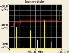
If the product is operating like an unlicensed and unwanted radio transmitter, it cannot be shipped. If designers ignore ringing and fail to implement a proper power delivery strategy, the radiated-EMI problem cannot be fixed through any method other than a complete board re-layout.
Susceptibility
Products will fail susceptibility tests and customer expectations if outside noise, such as static electricity discharge or strong radio signal fields, cause the product to fail or operate erratically. There are certain design characteristics that only apply to susceptibility but in general, proper stack up, appropriate power delivery, and effective EMI minimisation techniques also aid in creating bullet-proof designs.
How you really do it...
Triage signals
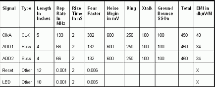
We must divide the signals into varying levels of criticality. I call this process triage. I break the signals up into clocks (or signals that look like clocks), busses, and other.
'Clocks' have fast rise times, high repetition rates and typically long trace lengths. This is the worst of all worlds for EMI. They are also the most critical of the signals because any type of ringing or non-monotonic nonsense can result in false clocking. Clocks are the primary contributor to radiated-EMI and must always be analysed quite rigorously.
'Busses' typically have fast rise times but a slower repetition rate than clocks. They can be long and have nasty ramifications if termination requirements are ignored. Since they can have multiple signals changing state simultaneously, busses are a significant contributor to radiated EMI and a primary contributor to ground bounce and SSOn.
'Others' are signals that may have fast rise times and long trace lengths, but since they have a very low repetition rate, they are generally inconsequential from a high speed system design stand point. In any case, designers need to use a spreadsheet tool like Excel to keep an orderly list of the various signals.
A useful way to sort signals for criticality is to multiply the length times by the repetition rate and divide by the rise time. This gives designers a number that gets big for high criticality signals and small for low criticality signals.
Budget noise, time, and EMI
Ringing, cross talk and ground bounce, as well as signal transit time and EMI contribution, must be budgeted. In the triage spreadsheet mentioned earlier, take the worst case ringing, plus the worst case crosstalk, plus the worst case ground bounce and add those numbers together. The total must be substantially below Vlow and above Vhi. It may seem that this worst case analysis is overly conservative. That may be, but ringing, crosstalk, and ground bounce are all vectors. It is not known when they add in phase and when they add out of phase. If they add in phase only once every billion times that means the product fails about once every five seconds. If that number is raised to once in a trillion (1 in 10e12), the average product glitches every 1,3 hours. There is no choice. Designers must design using worst case analysis. It should be noted that it is far easier to make a board that works reliably than it is to make a board that passes FCC/CISPR EMI specifications. Therefore I highly recommend keeping ringing, cross talk and ground bounce to an absolute minimum regardless of the margin available in the budget. It is necessary to make the same analysis for timing, noise, etc, on all clocks and busses or signals that display the characteristics of fast rise time and high repetition rate.
The problem is not in the budget. It is in accurately predicting how physical parameters affect the electrical performance of the finished board. You must accurately predict ringing, cross talk, ground bounce, and EMI as a function of the layout choices you have available. The more accurate the predictions, the more likely you are to achieve success on the first try.
These parameters can vary wildly and are dependent upon the actual layout. In many cases, terminations may be necessary in order to make a long trace behave properly. Using some type of proven reliable simulator is the only time effective way to get accurate answers. The alternative to simulation is to build a test board. If you decide to build a test board, remember to build an array of circuit layouts to bracket the behaviour of the circuit. In some cases you will have the benefit of a design guide. Some guides are good, some are bad, and some are absolutely horrible. I am adamantly against blindly using a design guide without understanding the physics behind their recommendations.
Develop a board stack up and power delivery system
There are two objectives behind this step. First you must provide for adequate controlled-impedance signal paths suitable for routing the high speed signals. Second you must develop a power delivery system which will hold the ground bounce below your budget and provide high frequency bypassing to help control common mode EMI conversion. The power delivery system includes the power supply, the bypass capacitors, and the power ground sandwich. The sum total of this array must provide low impedance power on the order of 0,1 Ω from DC to the highest frequency of interest. The highest frequency of interest for signal integrity reasons is Fknee or about 0,35/rise time. The highest frequency of interest for EMI reasons is 2/rise time or higher.
Develop clock strategy
Clocks must deliver a clear unambiguous transition that appears at all relevant devices within a specified window of time. The circuit designer must determine the physical constraints necessary to attain the electrical performance needed for the system to work reliably. To do that, the circuit designer needs to explore competing strategies and specify a topology that accomplishes the goal. Once having determined the physical characteristics necessary for success, that information must be recorded in the triage spreadsheet. Competing topologies and termination strategies will have their own set of sensitivities and radiated emission by-products.
When you physically lay out the clock, pay attention to the return current path. If you cannot see the obvious return current path by inspection, you are in grave danger of failure. Also pay attention to how close you route 'other' signals to the clock. Getting clock-based crosstalk onto an adjacent trace can easily cause FCC/CISPR radiated EMI failure. How close is too close? Designers need to know that answer.
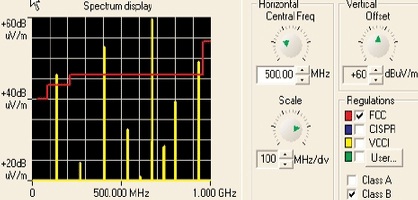
The clock EMI budget must be at least 6 db below the FCC/CISPR specification.
Develop buss strategy
It is important to know critical information before beginning layout and ask specific questions, such as:
* What is the maximum length in parallel before we exceed our crosstalk budget?
* What is the maximum length before we need to terminate the buss?
* If terminated, how should it be done?
* Can timing and skew requirements be met with a particular routing topology?
* How does this topology affect radiated EMI?
* If designers need to shift from one controlled impedance layer pair to another, how is it assured that there is an adequate return current path? In other words, part of the layout needs to be the structures which assures a clean return current path.
Begin physical board layout
Place components and validate Manhattan length
Once the layout designer has placed all the components in the high speed signal path on the board and prior to routing those signals, take a snapshot of the database and perform a ringing simulation using Manhattan (ie X Y) routing distance. If it appears that the length is too long to perform correctly, contact the layout designer and explain that they must:
1. Move the components closer together.
2. Route on a 45° angle layer to shorten the route within limits.
3. Add termination components.
The critical issue from a methods standpoint is to get the correct information quickly so the layout designer does not waste a lot of time on something that will not work.
Route clocks/busses and validate performance
The process of taking snapshots of a partially-completed board continues until all of the high speed critical signal paths are routed. The goal is to catch any problems early without slowing down the progress of the layout function. When all of the high speed paths are routed, perform full ringing, crosstalk, and EMI simulation. If the board meets the triage budget at this point and nothing gets changed later in the process, the system meets all high-speed design goals. The issue of 'will it work' is settled far earlier in the process. Conversely, if there is a problem, it can be fixed early in the process rather than wasting critical engineering resources and precious calendar days to first shipment.
Route everything and perform crosstalk check
The last detail to be analysed is the problem of crosstalk from high speed signals coupled on to an 'other' signal. 'Other' signals are the signals that are basically ignored because they did not have enough activity to warrant full analysis. Consider the problem of coupling a high order address signal on to the reset line. The board would work fine until you hit a high address range and then it would reset. Consider coupling the clock on to the line that drives the 'power on' LED on the front panel. The product would work, but would never pass FCC/CISPR regulator tests. The key to a happy life in the world of high speed system design is to get the right information early in the process and compare the predicted result with the actual result and correct the method/process if the predicted and actual results do not match.
Install filters on leads
The notion here is to simply follow best practices when using ferrites and filters. However, you cannot expect more than about 6db max. Hence if the basic design is not solid, users never get passed, simply relying on filters and shielding.
Conclusion
If you intend to pass FCC and CISPR test on the first pass, remember the following points:
* Make a rational budget for all signals of interest. Use something like the triage spreadsheet and keep track of your assumptions.
* Make a solid layer stack-up which provides for both controlled-impedance routing pairs as well as the power ground sandwich which provides the high frequency bypassing. Pay attention to the return current and the structures that will assure an unambiguous return current path.
* Simulate clocks and busses to assure that the layout constraints will add up to the electrical performance necessary for success. Remember that busses not only cause simultaneous switched output noise, but they can also add in-phase as far as radiated EMI is concerned.
* Begin layout, but validate the placement and high speed routing as soon as possible. There is no point in continuing to route a design that will not work.
* Prior to fabrication, do a final high speed path simulation to assure yourself that everything is correct.
* Last do a very rigorous crosstalk check to assure that no 'hot' signals are being coupled into an 'other' signal resulting in an unexpected EMI source.
Words of caution...
First, it should be obvious that I am a strong advocate of using a simulator to get the information you need to design high speed digital systems properly. I know of no other way to get the vital pieces of information necessary to get it right the first time and also provide the designer some notion of the manufacturing margin. I must, however, offer a word of warning when using any simulator. All of them depend upon a rational board stack-up which provides a reliable return current path as well as an adequate power deliver system. If either of these areas is deficient, the simulator will not reflect reality.
Second, this article is the condensed version of an 8-hour class. The 8-hour class was a condensed version of a 2-day class. Read this information as a set of rational ideas that hang together and have worked well in major corporations. Do not make the assumption that it is a rigorous document that has covered everything that is important. I highly recommend reading books like High-Speed Digital Design by Johnson and Graham or High-Speed Digital System Design by Hall, Hall, and McCall or Right the First Time by Ritchey. There are other good ones, but these are the ones I would start with. In addition, take training classes. Take multiple classes on the same subject from multiple instructors. If you are like me, you will always gain new insight when hearing the material from a fresh perspective.
Third, designing a power delivery system and analysing high speed paths for proper return current control may sound as exciting as watching paint dry, but it is critical for success. Become a board stack-up connoisseur. Spend the time to understand what this vital step means to both power delivery and to return current control.
About the author
Terry Fox has a BSEE from Montana State University 1969 and has spent 12 years with Hewlett Packard, three years with Daisy Systems, and the last 16 years in independent sales and consulting, and now spends the vast majority of his time teaching.
| Tel: | +27 11 315 8316 |
| Email: | [email protected] |
| www: | www.asic.co.za |
| Articles: | More information and articles about ASIC Design Services |


© Technews Publishing (Pty) Ltd | All Rights Reserved
 printer friendly version