


High precision and signal analysis applications such as scientific instruments, imaging systems, medical instruments and spectrum analysis require high-speed analog-to-digital converters (ADCs) with high integration, excellent noise performance and low power consumption.
Typically, applications such as these have used either a microcontroller (MCU) with a 12-bit ADC or a standalone 16-bit ADC and an MCU. However, these methods add complexity and cost to the system. A better alternative is to implement an 8-bit MCU with an integrated 16-bit ADC on-chip reducing the board space, power consumption, development time and system cost while increasing performance and reliability.
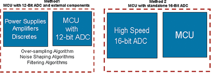
When designers use an MCU with an integrated 12-bit ADC, external operational amplifiers signal condition the input with a preamp gain of up to 16, which effectively provides four additional ADC bits to the measured signal. However, there are several disadvantages to using this method. When amplified, larger signals eclipse the input range of most ADCs. Many of these systems also need to use oversampling, noise shaping and software filtering techniques to achieve system performance goals, which adds to software development cost. However, if designers oversample and average, or decimate, to achieve higher resolution, throughput is reduced by a factor of the oversampling ratio forcing a trade-off between resolution and throughput for a given sampling rate. Another trade-off is the reduced processor bandwidth during each sampling period (1/fs) due to additional sampling and computations required to achieve the additional resolution.
Another way to achieve 16-bit resolution is to implement a low-cost MCU with a standalone high-speed 16-bit ADC. This approach offers accuracy, efficient real estate and is less complicated to design and debug than the first method. However, standalone high-speed ADCs are expensive, which increases the overall cost of the system. A standalone ADC is typically very power hungry and is not appropriate for applications that require low power.
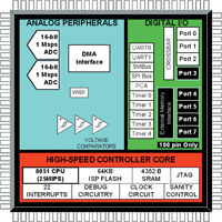
The third and best option for solving the problem of signal conditioning is to replace an MCU and a standalone ADC with a fully integrated mixed-signal MCU. For example, the C8051F064 MCU integrates dual 16-bit successive approximation (SAR) ADCs. Each of the ADCs can be used as a single-ended channel giving one mega sample per second (Msps) each or interleaved to provide a maximum of two Msps. These low-noise ADCs dissipate only 20 mW per channel offering the lowest power ADCs with comparable performance levels to standalone ADCs. Another advantage of the ADCs is their high-accuracy of 0,75 least significant bit (LSB) integral non-linearity (INL) and a signal-to-noise ratio of 89 dB SINAD. Due to the high sample speed, a direct memory access (DMA) is integrated that allows results to be transferred to RAM or a parallel port.
The C8051F064 family also has a high-speed, pipelined 25 MIPS 8051 CPU. Proprietary advanced design and verification methodologies enabled a 'hard-wired' implementation of the C8051Fx CPU to maximise the instruction throughput while retaining complete object code compatibility. On-chip digital peripherals include 64 KB of Flash memory, 4352 bytes of RAM, two standard UART, SMBus and SPI serial interfaces. The digital peripherals are mapped to the I/O pins via a crossbar that routes the required digital functions to the pins.
An on-chip 2% precision internal oscillator allows for increased integration and external component elimination. The 24,5 MHz oscillator eliminates the need for an external precision crystal oscillator or resonator, which can save $0,50 to $1 in many systems. The oscillator, which is calibrated at the factory, is also accurate enough to generate the communication clock for the standard UART baud rates. Port pins can be configured to accommodate a tighter tolerance oscillator if required. By running the oscillator at a lower frequency, customers can lower the overall power consumption of the system. By cutting the master clock's frequency in half, the operating current is approximately cut in half. The C8051F064 product supports four divide down (up to a divide by eight) master clock modes.
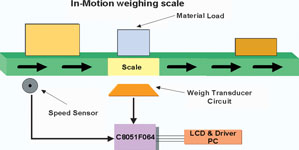
For example, an application that is easily simplified using an MCU with an on-chip, high-speed 16-bit ADC such as the C8051F064 is an in-motion weigh scale. These extremely fast and efficient scales offer highly accurate package weighing but require high-speed analog and processing capability to gather and process the weight data because the speed of the conveyor belt is extremely high. Under this circumstance the 1 Msps, 16-bit SAR ADC has a shorter sampling time and therefore greater measurement accuracy versus delta sigma ADCs, whose accuracy drops off as throughput increases. A high-speed CPU is required to process the data very quickly with an algorithm running at high speed.
A typical in-motion weigh scale is shown in Figure 3. A bridge transducer supported on load cells, high-performance MCU and a belt-speed sensor are the main components of the system. Material weight on the belt is measured by load cells that send a voltage signal to the ADC proportional to the force applied to the bridge. To determine an accurate weight, the high-speed ADC constantly samples the load cell output from when the package enters the weigh station conveyor until the package is completely over the scale. The samples collected at this point are averaged to obtain a final weight value. This data can be displayed either on the LCD panel or transmitted through a standard serial port to a PC for further analysis and reporting.
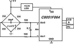
Bridge transducers are the most common sensor type in an in-motion weigh scale. They convert a force into a voltage that is proportional to the force applied to the bridge. Bridge transducers are used because they are extremely linear and have repeatable characteristics for large applied forces. The full-scale output voltage of this type of sensor depends on its excitation voltage (the voltage used to excite the sensor). 5 V is a common excitation voltage. For example, a five pound scale that has a bridge transducer with a 10 mV/V sensitivity excited with a 5 V supply will ideally produce a 50 mV output voltage when a five pound weight is placed on the transducer.
The modern way to resolve such an analog signal is to use an (ADC), in this case a 16-bit ADC, with an LSB that is smaller than the signal to be resolved. A common full-scale range for most ADCs today is 2,5 V, which is set by the voltage reference of the system. The 16-bit LSB with a 2,5 V reference is 38 μV. This signal amplitude would allow 1315 division of the 50 mV full-scale output signal, providing enough accuracy for this kind of application.
In this example, the 16-bit ADC's 38 μV (2,5 V VREF) LSB provides significant overhead to account for system issues such as temperature drift and offset error. When designing this system, design engineers should consider other parasitic board level issues like amplifier noise drift and parasitic thermocouple effects on the system board.
Figure 4 illustrates a C8051F064-based in-motion weigh scale. The F064 provides a low-cost system-on-chip solution for this application. Using the F064, the entire measurement system can be implemented using a bridge transducer, a low pass filter, an LDO, a serial PC connection, an LCD driver and an LCD. This integrated solution eliminates the need of oversampling techniques and signal conditioning circuit to improve the performance of the ADC.
When using a C8051F064 in an application such as an in-motion weigh scale, the analog data conversion and system support functions are integrated into a single package providing lower power consumption and higher accuracy. By including high-precision, high-speed analog peripherals with digital control circuits on the same chip, the C8051F064 allows designers to bypass system level analog-digital integration issues and provide a host of benefits that cannot be found using any other solution.
| Tel: | +27 11 608 0144 |
| Email: | [email protected] |
| www: | www.nuvisionelec.com |
| Articles: | More information and articles about NuVision Electronics |


© Technews Publishing (Pty) Ltd | All Rights Reserved
 printer friendly version