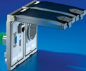
Interface flaps provide optimum data and supply connection for enclosures
7 September 2005Manufacturing / Production Technology, Hardware & Services
Enclosures, machinery, and equipment often require connections to external devices like laptop, programming devices, or diagnosis units.
The new modular interface flap that Rittal offers allows for quick connection of controls, data lines and switches. The installation of the interface flap at the enclosure panel avoids unnecessary detours and improvised cabling solutions. As the enclosure or the housing remains closed, the prescribed type of protection for the installed components remains intact.
The interface flap features integrated latching and meets safety class IP65 requirements. This prevents the ingress of dust and moisture. The modular design affords a maximum of flexibility because the mounting frames can be fitted with a comprehensive product range of data rack connector sets and socket modules - ranging from socket outlets with earthing contact, to Ethernet connections - simply by snapping in. This allows individual modification and updating at any time.
The interface flaps are also characterised by a high degree of mechanical ruggedness and temperature resistance. They are available made as precision zinc casting, matt nickel-plated or, alternatively, with plastic flap and polycarbonate locks, transparent. They are available as single or twin version: 65 x 120 mm or 130 x 120 mm.
World-first 016008 mm component placement
Manufacturing / Production Technology, Hardware & Services
Fuji has achieved the world’s first placement of 016008 mm (0,16 x 0,08 mm or 006 x 003 inches) size components on printed circuit boards with its SMT pick and place machine, NXTR.
Read more...Lifecycle and obsolescence: Protecting electronics through process Production Logix
Manufacturing / Production Technology, Hardware & Services
At Production Logix, we believe longevity is not accidental. It is engineered through early visibility, structured response, and disciplined execution, in partnership with our OEM customers.
Read more...Maximising squeegee quality and durability Testerion
Manufacturing / Production Technology, Hardware & Services
Transition Automation has announced two new product advancements designed to improve SMT printing performance and extend squeegee life: laser-enhanced Permalex bonding and integrated edge protectors.
Read more...NeoDen ND2 PCB screen printer ZETECH ONE
Manufacturing / Production Technology, Hardware & Services
The NeoDen ND2 PCB screen printing machine is a fully automatic stencil printer designed to deliver precise and consistent solder paste application in modern SMT production environments.
Read more...Understanding the BGA rework process Techmet
Manufacturing / Production Technology, Hardware & Services
BGA rework is a highly technical process that involves removing the faulty component, preparing the circuit board, and installing a new or repaired device, while maintaining the integrity of the printed circuit board.
Read more...Flexible three-process reflow soldering system Truth Electronic Manufacturing
Manufacturing / Production Technology, Hardware & Services
By combining multiple soldering technologies within a single system, the Vision TripleX system enables manufacturers to adapt easily to different assembly requirements, board designs, and production volumes.
Read more...Inline vapour phase soldering for high-volume production MyKay Tronics
Manufacturing / Production Technology, Hardware & Services
The VP2200-100 vacuum inline vapour phase soldering system from ASSCON is designed for fully automated, high-volume electronics manufacturing where process consistency and solder joint quality are critical.
Read more...Global electronics solutions since 1964 IMP Electronics Solutions
Manufacturing / Production Technology, Hardware & Services
Over more than six decades, IMP Electronics Solutions has built a reputation for technical expertise, reliable supply chains, and strong partnerships with both customers and manufacturing partners.
Read more...Driving excellence in electronics manufacturing Jemstech
Editor's Choice Manufacturing / Production Technology, Hardware & Services
Jemstech’s reputation for disciplined execution and client-focused service has earned it strong loyalty from companies operating in demanding industries.
Read more...When do you need Nitrogen in reflow? Truth Electronic Manufacturing
Manufacturing / Production Technology, Hardware & Services
Nitrogen in reflow soldering is often seen as a performance enhancer, offering improved wetting, shinier joints, and fewer defects. But it is not always necessary.
While every effort has been made to ensure the accuracy of the information contained herein, the publisher and its agents cannot be held responsible for any errors contained, or any loss incurred as a result. Articles published do not necessarily reflect the views of the publishers. The editor reserves the right to alter or cut copy. Articles submitted are deemed to have been cleared for publication. Advertisements and company contact details are published as provided by the advertiser. Technews Publishing (Pty) Ltd cannot be held responsible for the accuracy or veracity of supplied material.


 printer friendly version