


The factorised power architecture (FPA), in concert with IC-style chip devices, provides power system designers with high performance at low cost. FPA is enabled by the power conversion chips, which efficiently process over 200 W of power in a power ball grid array with power densities over 800 W/cubic inch.
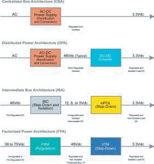
Distributed power has been a viable design approach for decades, albeit almost exclusively in the telecommunications domain. Board-mounted DC-DC converters, for example, were constructed with discrete components and used to convert power from a centralised supply to more usable power, typically at a backplane. Subsequently, the advent of high-density DC-DC converter modules paved the way to more widespread use of the idea in EDP, industrial, military, and medical applications. Since that time, the chorus of articles in the trade press extolling the virtues of distributed power architecture has been increasingly loud and clear: centralised architecture is going or gone and DPA is king. The structure and operation of each of these power architectures is summarised in Figure 1, and they are discussed in subsequent paragraphs.
Centralised architectures
The evolution of power architectures began with the centralised architecture. A centralised power supply contains the entire power supply in one housing - from the front end through the DC-DC conversion stages. It converts the line voltage to the number of DC voltages needed in the system and buses each voltage to the appropriate load. It is very cost effective. It does not consume precious board real estate at the point of load with the power conversion function. It is relatively simple to manage thermals and EMI. It is fairly efficient because it avoids serial power transformations. In the past, the centralised system, usually a custom design constructed of discrete components, was often chosen because it was less expensive. These systems, in general, work well when the power requirements, once defined, are not likely to change and space is not an issue.
The central supply should be located near the load to minimise I²R losses, and it should also be located as close as possible to the AC entry point to reduce noise radiated from the unshielded AC lines. This is often a difficult trade-off, with the input cables requiring shielding to minimise common and differential mode currents that produce noise.
Centralised power works well in many respects, but the most obvious problem is how to distribute hundreds of amps common with low output voltages. Centralised power also lacks scalability. Many systems can be configured with varying numbers of PC cards representing widely varying loads (eg, line cards in a PBX). With centralised power, the power supply must be sized to handle the maximum configured system, which could put the small configurations at a cost disadvantage.
What is more, the remoteness of the supply from the load can negatively impact the ability of the supply to react to a rapidly-changing load (ie, transient response). Also, thermal management can be a special challenge in a centralised architecture, where excess heat could amount to hundreds of watts all in one concentrated area. Large heat sinks and fans are often needed to keep the power supply from becoming overheated. System hotspots are a source of reduced reliability.
Distributed power architecture
Distributed power architecture (DPA) addresses some of the shortcomings of a centralised architecture. Distributed power is a decentralised power architecture usually consisting of an AC-DC converter at the AC mains serving DC-DC converters located elsewhere. The AC-DC converter might provide regulation, isolation, noise suppression, and power factor correction as well as an intermediate DC voltage, frequently 48 V. This intermediate voltage is converted by DC-DC converters located at the point of the load they serve. Typically, power in a telecom system is distributed on a 48 V bus. On-board isolated DC-to-DC converters are matched to the load requirement. This helps with dynamic response and eliminates the problems associated with distributing low voltages around the system. DPA was actually enabled by the development of high-density bricks.
A distributed approach spreads the heat throughout the system, greatly reducing or eliminating the need for heat sinks or high velocity airflow. With temperature more evenly maintained throughout the system, reliability specifications are easier to meet.
DPA, however, can be more costly in a number of ways. For example, isolation, regulation, transformation, EMI filtering, and input protection are all done at every brick. And coming from an offline source, rectification and conversion to the distributed bus voltage are needed - so that is an additional power-processing step that reduces overall system efficiency.
Furthermore, if a single DC-DC converter cannot provide adequate power or fault tolerance for a particular output voltage, multiple DC-DC converters will need to be paralleled, creating additional complexity owing to the need to connect remote-sense leads from each paralleled converter to a single, common, point and the need for additional circuitry within each paralleled converter, to force power sharing among the units.
Intermediate bus architecture
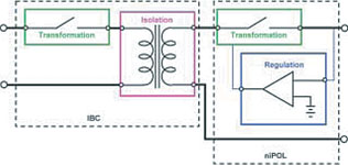
The intermediate bus architecture was first to separate the DC-DC converter functions of isolation, transformation, and regulation and allocate them to two devices. The IBC (intermediate bus converter) provides intermediate voltage transformation and isolation and the niPOL (non-isolated point of load) converter provides final transformation and regulation.
IBA can be a very cost-effective solution because point-of-load converters do not require any isolation and tend to be a lot less expensive. Non-isolated POL converters within the intermediate bus architecture forego isolation and high ratio voltage transformation to improve cost-effectiveness, but they depend upon a nearby bus converter to supply power at a low input voltage. On the negative side, the lack of isolation in niPOL converters make over-voltage sensitive loads vulnerable to deadly faults and the entire system vulnerable to potential ground loop problems.
The intermediate bus converter introduces a power-processing step to go from, say, the 48 to 12 V that intrinsically reduces efficiency of the system. Also, the bus converter really does need to be located close to the load, because even at 12 V, fairly high currents need to be moved around the board so large traces or short runs are needed. The 12 V bus itself is a bit low for efficient distribution of a lot of power. But it is too high to step down to a very low voltage because of the very low duty cycle on the switch. As a result, it is difficult to make a highly efficient IBA system.
Factorised power architecture
Factorised power architecture (FPA) also separates conventional converter functionality into two power building blocks. This new architecture, in concert with IC-style chip devices (see Figure 1), provides power system designers with high performance at low cost. FPA is enabled by the power conversion chips, which efficiently process over 200 W of power in a small (less than 4 cm³ and light (less than 13 grams) power ball grid array (BGA) or J-level package, with power densities over 49 W/cm³. These functional building blocks are deployed as surface mount (SMD) components to create a flexible factorised power system.
One building block, the pre-regulator module (PRM), is designed to accept a wide-range supply voltage and convert it to a factorised bus - a controlled voltage source - with 97% to 99% efficiency. Another building block, the voltage transformation module (VTM), is designed to convert the factorised bus to the voltage levels required by the load with efficiencies as high as 97%. The VTM will also provide input-to-output galvanic isolation.
The combination of FPA and IC chips give the power designer the flexibility to use only what is needed where it is needed. The minimal complement of PRMs and VTMs depends upon the multiplicity of outputs, power levels, individual regulation and power system fault tolerance requirements. VTMs and PRMs may be paralleled with accurate sharing for higher power or redundancy; in fact, VTMs inherently current share when inputs and outputs are paralleled. This avoids the need for a power-sharing protocol, interface signals and a multiplicity of remote sense connections.
By exploiting a zero-voltage switching and zero-current switching topology, the VTMs limit the common-mode and differential-mode noise at the point of load. For example, the output of a VTM configured to convert 48 V to 12 V exhibits about 12 mV p-p of high-frequency ripple with just 1 μF of bypass capacitance. That noise voltage amounts to only 0,1% of the DC output.


© Technews Publishing (Pty) Ltd | All Rights Reserved
 printer friendly version