


Power converter design is a multidisciplinary process; an effective designer needs to understand analog and mixed-signal circuit design, wound components, electromagnetic compatibility, packaging, and thermal design. Packaging and thermal design are driven by increased power density and the many trade-offs in power topology selection. The challenging environment in equipment destined to power the expanding information infrastructure brings thermal design into sharp focus.
The world of modular DC-DC converters or 'bricks' is evolving at a rapid pace since the first full-brick was commercialised in the mid-eighties. For instance, the sixteenth-brick format is 7,74 cm² of PCB area with a staggering 33 W to 50 W throughput.
The telecom bus operates over a wider range, 36 V to 72 V, than its datacom counterpart that has a tighter tolerance. A bus converter converts this bus with isolation at each card (the first use of the brick format). The on-card power is then applied directly to the load circuits. However, in recent years the proliferation of DSP and digital ASICs has spawned an intermediate bus architecture in which the bus converter delivers an isolated 12 V to 14 V, which is further converted by point-of-load regulators, physically located at the loads on the card.
Once the power supply designer has selected the topology to match the application, considered the number of power conversion stages and whether the converter is hard- or soft-switched, then the switch and rectifier selection takes centre stage. Most bricks employ power MOSFETs for the power switches and low-voltage synchronous rectifiers. MOSFET technology has evolved considerably, presenting the designer with trench devices with benchmark RDS-ON and planar devices with low inter-electrode capacitance. Device selection, once the voltage and current rating has been established, depends on which characteristic, switching speed or RDS-ON dominates the loss. In recent times, the ratio of CDG to CGS has influenced designers as an indicator of the likelihood of shoot-through in high-power, high-frequency, half-bridge power stages.
Switching frequency and EMI trade-offs
A perennial trade-off is that of switching frequency with efficiency and electromagnetic interference. Switching losses in the power switches, rectifiers and control circuitry increase with switching frequency. In modular DC-DC converters, increasing frequency is desirable as it drives down the size of the filter and energy storage components. However, in hard-switched applications, the increased high-frequency harmonic content in the power devices results in larger displacement currents in the stray capacitances between devices and heatsinks or power planes, and through the interwinding capacitance of transformers. Such displacement currents manifest themselves as common-mode interference.
In DC-DC converter control and drive applications, IC design and packaging has embraced the challenge presented by the brick environment. At the circuit design level, increased integration, in-board, high-voltage regulators, higher clock frequencies and low shoot-through drivers with programmable slew rate are available for new designs. A key issue in power IC design is that of thermal regulation. Power ICs have integrated drivers, regulator pass transistors and power switches arranged at the periphery of the die next to the bond pads. As these devices operate, heat conducts through the body of the die creating a thermal 'map' with isotherms (contour lines of constant temperature). Certain sub-circuits, particularly differential circuits where matching is critical, are adversely affected if the individual transistors are positioned on different isotherms. IC layouts must be adjusted such that transistors in such applications see the same temperature, at the same time, when the device is operating, which is not a trivial task. Photomicrographs of power ICs often reveal devices that are cross-coupled for first-order cancellation of thermal effects.
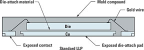
The LLP leadless leadframe package, shown in Figure 1, is a leadframe-based chip scale package (CSP) that enhances chip speed, reduces thermal impedance, and reduces the PCB area required for mounting. The small size and very low profile make this package ideal for the high component density, multilayer PCBs used in modular DC-DC converters.

The LLP has the following advantages:
* Low thermal resistance.
* Reduced electrical parasitics.
* Improved board space efficiency.
* Reduced package height.
* Reduced package mass.
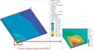
IC package design is a painstaking process involving extensive thermal and mechanical modeling coupled with fabrication and measurement stages in which finite element models (as shown in Figure 2) are compared with spot measurements on the die or by thermal imaging. Generally, spot measurements on the die are accomplished by measuring the forward drop of a diode in a test die incorporated within the new package. This tried and tested technique is used in many of the remote diode temperature-sensing devices that protect the latest generation of microprocessors, DSPs and digital ASICs. One or more diodes in the test die may also be used to inject heat to verify the thermal characteristics of the die.
Package design and thermal properties
Thermal properties of electronic packages are characterised by θJA and θJC. θJA can be defined as an overall package thermal resistance, which is the sum of package internal and external thermal resistance. It can be expressed as:
θJA = θJC + θCA = (TJ - TA)/P
Where:
θJC: (TJ - TC)/P, junction-to-case conductive thermal resistance (°C/W)
θCA: (TC - TA)/P, case-to-ambient convective thermal resistance (°C/W)
P: I (current) x V (voltage), device heat dissipation (W)
TJ: Average device junction temperature (°C)
TA: Average ambient temperature (°C)
TC: Case temperature at a prescribed package surface (°C)
θJC is dominated by the conductive thermal resistance within layers of packaging materials, and is highly dependent on the package configuration. If the heat flow is assumed to be perpendicular to each layer of the packaging material, θJC may be expressed as:
Σti</FONT>/(ki</FONT>Ai</FONT>)
Where ti</FONT>, ki</FONT>, and Ai</FONT> are the thickness, thermal conductivity, and heat transfer surface area of each packaging material layer, eg, die-attach material, lead frame, die coating, and encapsulant or mould compound.
θCA is the external convective thermal resistance. It is greatly affected by adjacent ambient conditions, package boundary conditions, and conjugate heat transfer. In the LLP, low junction to ambient thermal resistance is primarily affected by reducing the resistance from the thermal plane on the PCB to the junction. The cross-section in Figure 3 shows that the die is soldered to the die-attach pad, which is directly soldered to the power plane on the PCB. The area of the PCB power plane dominates θCA, in brick applications where conduction is the primary method of heat transfer and convection cooling is restricted due to the diminishing pitch between cards.
Packaging comparisons
The θCA may be improved by utilising thermal vias in the power plane under the device. This improvement is second order compared with that achieved by increasing the area of the plane to which the LLP is soldered. A comparison between the LLP and a conventional small-outline package with the same pin count and die reveals the benefits.
Let us take an MSOP-8, where the PCB area is 15 mm² compared to an LLP-8 which is 9 mm². The dramatic difference is in the thermal resistance where the LLP-8 exhibits a thermal resistance (θJC) of 40°C/W versus 200°C/W for the MSOP-8.
In conclusion, a modular DC-DC converter is a most demanding environment for power ICs. The inexorable push to higher power density and the necessity for higher-efficiency drives power IC and package designers to set new standards in thermal resistance and volumetric efficiency. Giving power supply designers a brief glimpse into the package design, measurement and verification process is an important part of launching a new standard, particularly in power applications where new discrete power packages are a frequent part of the landscape.
For more information contact Simon Churches, Arrow Altech Distribution, +27 (0)11 923 9600, [email protected]
| Tel: | +27 11 923 9600 |
| Email: | [email protected] |
| www: | www.altronarrow.com |
| Articles: | More information and articles about Altron Arrow |


© Technews Publishing (Pty) Ltd | All Rights Reserved
 printer friendly version