


Ref: z2920154m
Baluns (balanced to unbalanced) are used in push-pull amplifiers to provide signal splitting and/or combining and 180° phase shifting. Although their usage and design is well known, mainly for broadband amplification, with the recent arrival of high power LDMOS MMICs in the cellular base station arena, and the subsequent reduction in component count, no attempt has been done to integrate on the particular substrate used by LDMOS RFICs this functionality.
This article deals with the LDMOS IC substrate specifics, the balun design challenges, and presents two successful designs and the associated measurement data.
Background
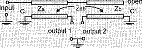
The simplified topology of a push-pull amplifier is presented in Figure 1:
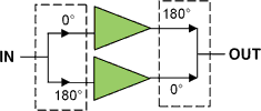
The two dotted lines rectangles represent the input and output balun functions.The input balun splits the RF signal in two, creates a 180° phase shift between the two signals, and can create (if desired) a broadband matching structure, therefore decreasing the transformation ratio between the generator (50 Ω) and the transistor terminal. The output balun has an opposite role, it combines the two signals while out-phasing them, and also can provide a broadband matching structure. The two transistors amplify in-phase opposition. Among the different advantages of a push-pull configuration, is the bandwidth performance, resulting from a lowered transformation ratio between transistor terminals and load, compared to a single-ended configuration.
In recent years, in the RF power basestation world, many RF semiconductor manufacturers have introduced integrated power amplifiers using laterally diffused metal oxide semiconductor. All these components are aiming at narrow-band amplification and therefore feature a single-ended topology.
One of the characterisitics of the LDMOS technology is the use of very low resistivity substrate, of the order of tens of milliΩ-cm. This feature, although highly desirable from the transistor standpoint for source grounding purposes, is a real nightmare in terms of passives - mainly inductors and transmission lines that suffer from very low quality factors. The reported activity in this article relates in general to the design of broader band amplifiers than conventional 5% relative bandwidth single-ended power amplifiers, using push-pull structures with specific emphasis on the input balun circuits, in LDMOS technology.
Balun designs
The targeted bandwidth for the balun is 1,8–2,7 GHz with appropriate amplitude and phase unbalance, and insertion loss compatible with the achievement of a reasonable gain for a two stages LDMOS RFIC (25 dB).
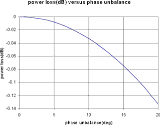
Let us consider the impact of amplitude and phase unbalance on the power loss of a push-pull power amplifier. We shall assume that two signals v1(t) and v2(t) are applied on the balanced port of a balun and v(t) is the resulting signal at the output on the unbalanced port.
Phase unbalance:
V1(t) = V.cos(w1.t)
V2(t) = V.cos(w1.t + ΔΦ)
Therefore
V(t) = 2V.cos(ΔΦ/2).cos((2w1.t + ΔΦ)/2)
And the power loss due to the phase unbalance becomes
Power_loss = cos^2(ΔΦ/2).
This is illustrated in Figure 2:
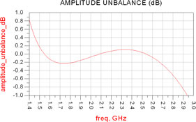
Amplitude unbalance:
V1(t) = V1.cos(w1.t)
V2(t) = V2.cos(w1.t)
Therefore
V(t) = (1 + V1/V2).cos(w1.t)
And the power loss due to the amplitude unbalance becomes
Power_loss = (V2/V1)^2
This is illustrated in Figure 3:
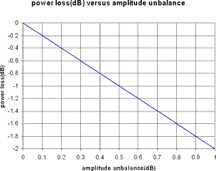
As demonstrated by these graphs, the amplitude unbalance has much more impact and is much more stringent than the phase unbalance.
Several active circuits have been considered, among them are the circuits using the 'natural' outphasing between drain and source, and differential pairs. For the frequencies of interest, with today’s available RF LDMOS transistors, the performance in terms of unbalance is not good enough, mainly because of excessive parasitic capacitances.
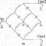
Among the passive structures, several circuits have been simulated, and some of them such as 'rat-race', or first order lattice balun, have been rejected because of insufficient bandwidth performance. Nonetheless, two of them have been considered, the second order lattice balun[1], and the Marchand type balun[2].
The former is based on the principle of two paths having respectively + and – 90° phase shift, achieved with low and high pass networks. This is illustrated in Figure 4. The latter uses the vertical coupling between transmission lines and the opposite current flow on the balanced sides creates the broadband 180° phase shift.
The principle is described in Figure 5:
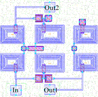
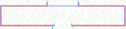
The lattice balun has been realised with conventional integrated inductors and capacitors, as shown in Figure 6, and the Marchand type balun is using the coupling between microstrip lines on different metal layers, and the layout is shown in Figure 7.
The lattice balun has been simulated with a conventional circuit simulator, while the Marchand balun required 2,5D electromagnetic simulation.
Experimental results
The two circuits above have been measured as standalone 3-port networks and also in cascade (as two ports) in order to measure the insertion loss. The results are presented in the Figures 8 through 13:
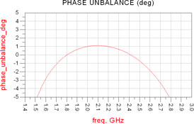
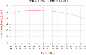
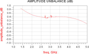
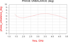
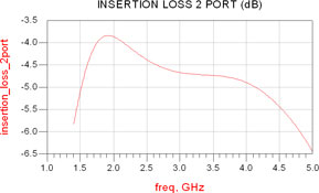
These measurements show that the second order lattice balun performs well in the 1,7–2,7 Ghz with 0,2 dB amplitude unbalance, 5° phase unbalance and about 2 dB loss. The Marchand balun has an even wider bandwidth, approximately 1,7–4 GHz with about 0,4/0,5dB amplitude unbalance, 6° phase unbalance and 4,5 dB loss. Although these insertion loss numbers are much higher than their semi-insulating or dielectric counterparts, these performance level remains highly compatible with the design of 25 dB and above two stages LDMOS MMICs (including the balun integration).
Conclusion
The present paper describes the need for integrated baluns in LDMOS IC technology, the design challenges linked mainly to the substrate limitations, and presents two functional circuits such as a second-order lattice balun and a Marchand type balun. The measured performances confirm the possibility to integrate such functions and may constitute a step towards power amplifiers for software definable radio.
References:
[1] D. Kuylenstierna, ‘Design of Broadband Lumped Element Baluns’, 2004 IEEE MTT-S International Microwave Symposium Digest; [2] N. Marchand, ‘Transmission-Line Conversion’, Electronics, December 1944, pp 142-145.
For more information contact Norman Ballard, +27 (0)21 554 3922, Freescale Semiconductor, [email protected]


© Technews Publishing (Pty) Ltd | All Rights Reserved
 printer friendly version