


In many applications, the power supply voltage is often dictated by an external design constraint such as battery voltage, bus-powered USB or something as mundane as a single-output, low-cost wall wart.
Unfortunately, these are also the applications that usually have a requirement for an additional supply that is not compatible with VDD. If the additional supply is lower, then an LDO solves the problem, but if it is higher, we have to go to a switcher.
In this article from microSOLUTIONS, Microchip Technology's Keith Curtis, shows an example of how some of the on-chip peripherals in a microcontroller can be used to create an impromptu switching regulator
While Microchip does make a line of switching regulators that fill this need quite nicely, there are some applications in which it is preferable to build the switcher out of peripherals built into the microcontroller. For this example, we will take a look at a simple hysteresis-feedback boost circuit using a comparator and the PWM function in a CCP (capture, compare, and PWM) module. The boost topology is used to generate a higher output voltage than the source voltage - so in this example, we are generating a supply voltage greater than VDD. The CCP modules that are found on many of Microchip's microcontrollers are used primarily for the measurement and control of time-based pulse signals.
Requirements
To build a switching regulator, you need a few things: a power switch, an inductor, a capacitor, a gated pulse generator, a voltage reference and a feedback path. In this example, the CCP will be our pulse generator, the 0,6 V comparator reference will be our voltage reference, and the comparator will be our feedback.
Figure 1 shows the circuit for our switching power supply, using the comparator and the CCP in PWM mode. The CCP generates the switching pulse, which turns on/off the switch Q1. D1 acts as the second half of the switch, connecting the inductor to the output during the discharge portion of the cycle. C1 accumulates the current flow from the inductor, smoothing out the pulses into a DC level. R1, R2, the comparator and the 0,6 V reference form the feedback path. When the divided output voltage is less than 0,6 V, then the comparator allows pulses from the CCP through the resistor to turn Q1 on. If the divided output is greater than, or equal to, the 0,6 V reference, the comparator shorts out the pulses by grounding the gate through a diode, and preventing the system from generating too high an output voltage. Figure 1 shows the waveforms generated both when the system has a low output, and when the system is at the desired voltage.
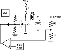
Note: (a) the pull-down resistor on the gate of the MOSFET is to hold the transistor off until the microcontroller configures the CCP and comparator. (b) if the CCP has the auto-shutdown feature, the resistor on the output of the CCP and the diode on the output of the comparator are not required, and the output of the comparator is connected to the CCP internally.
Calculations
Now, given that we have the circuit, we have to calculate a few component values. The first is the duty cycle of the boost circuit, which is determined by the source and output voltages. Equation 1 determines the minimum duty cycle required. Note that the duty cycle can be, and should be, a little larger than the value determined by Equation 1. The process of skipping pulses, based on the feedback, will reduce the average duty cycle to the optimal value when the system is running.
DutyCycle ≥ 1 - (VDD/VOUT) ……….[1]
The next value to determine is the inductance of the inductor; to simplify the calculation, we will first determine IRIPPLE, and then the size of the inductor. Equation 2 determines the necessary ripple current to keep the inductor current discontinuous (the inductor current goes to zero during the pulse cycle).
IRIPPLE = (2 x IOUT-MAX)/(1 - DutyCycle) ……….[2]
Given IRIPPLE, Equation 3 determines the necessary inductor value given the input voltage, the desired output voltage, the desired output current, and the switching frequency. One thing to note about the switching frequency (FSWITCH), it should be above 30 kHz to keep it inaudible and below 250 kHz to give a reasonable resolution for the PWM duty cycle (≤ 6,25%, assuming Fosc = 4 MHz)
Inductor = (VDD x DutyCycle)/IRIPPLE x FSWITCH) ……….[3]
The inductor chosen for the design should also have a saturation current at least two times IRIPPLE to prevent saturation and the violent failure of the MOSFET transistor.
The third value is the capacitance of the output capacitor C1. This capacitor acts as a filter, smoothing the pulse currents delivered from the inductor, into a DC voltage. To calculate the value, we need to know the maximum allowable output voltage ripple for the circuit. As this is determined by the load, the value must be supplied by the designer. Using this value, Equation 4 will determine the minimum capacitance required.
C1 ≥ (IRIPPLE x VRIPPLE)/(2 x Pi x FSWITCH) ………. [4]
One note on C1, while electrolytic capacitors are less expensive than Tantalum capacitors, electrolytic capacitors begin to act inductive above 50 to 100 kHz. If the switching frequency is much above 30 to 50 kHz, the added cost of the tantalum is often necessary to reduce switching noise in the output.
Three final choices must be made in the design; the minimum ratings for Q1 and D1, and the two resistors R1/R2.
Q1 should be rated for 2 x IRIPPLE and the gate charge QTOT should be kept as small as possible. If it is over 20-50 nC, or the source voltage to the boost circuit is greater than VDD, it will be necessary to use a MOSFET driver to boost the gate drive current/voltage. A low gate drive will result in the MOSFET transistor spending a large portion of each cycle in its linear region and that will drop efficiency and heat the transistor. Likewise, the current rating for the diode should be rated for 2 x IRIPPLE.
R1 and R2 form a voltage divider, and are chosen to produce a feedback voltage of 0,6 V when the output voltage of the circuit is at the desired voltage. See Equation 5.
R2 = ((VOUT - 0,6 V) x R1)/0,6 V ……….[5]
Summary
So, with a little maths, a few components, and a spare peripheral or two, it is possible to generate a supply voltage greater than VDD. More information can be found at Microchip's 'Intelligent Power Supply Design Center' at www.microchip.com/power.
For more information contact Arrow Altech Distribution, +27 (0)11 923 9600, Avnet Kopp, +27 (0)11 809 6100, Electrocomp, +27(0)11 458 9000, Future Electronics, +27 (0)21 880 0727 or Tempe Technologies, +27 (0)11 452 0530.
| Tel: | +27 11 923 9600 |
| Email: | [email protected] |
| www: | www.altronarrow.com |
| Articles: | More information and articles about Altron Arrow |
| Tel: | +27 11 458 9000 |
| Email: | [email protected] |
| www: | www.electrocomp.co.za |
| Articles: | More information and articles about Electrocomp |
| Email: | [email protected] |
| www: | |
| Articles: | More information and articles about Tempe Technologies |
| Tel: | +27 21 421 8292 |
| Email: | [email protected] |
| www: | www.futureelectronics.com |
| Articles: | More information and articles about Future Electronics |


© Technews Publishing (Pty) Ltd | All Rights Reserved
 printer friendly version