In this article Xilinx provides a functional description of Verilog source code for a keypad scanner. The code is used to target the lowest density, 32-macrocell CoolRunner-II XC2C32A CPLD device in a CP56 package (6 x 6 mm). The keypad accommodated in this design has eight rows and eight columns.
The design can easily be scaled to target keypads with more or less rows/columns. For instance, a keypad with seven rows and seven columns would allow the design to fit in the smallest QFG32 package (5 x 5 mm).
As handheld devices such as cellphones pack more and more features into them, they require more effective ways of entering data. Most cellphones, for example, use the standard DTMF style keypad and a multitap process to enter alphanumeric data; however, for larger amounts of data, multitapping becomes cumbersome. More and more high-end phones are therefore employing QWERTY keypads that make entering data easier and quicker.
Going from a DTMF to a QWERTY keypad requires more I/O. For instance, a DTMF keypad might have four rows and three columns, where a QWERTY keypad might have eight rows and eight columns. This can vary depending on the requirements.
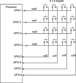
Typically, a processor (or ASIC) is used to interface to the keypad's rows and columns. The processor scans the rows and monitors the columns for a logic change. When a change occurs, it indicates that one of the buttons in that column was pressed. By knowing which row was being scanned, and which column changed state, the processor can deduce which specific button was pushed. Additional functions such as debounce are also typically employed. Figure 1 shows how a simple 4 x 4 keypad uses 8 GPIO of a processor.

Expanding I/O
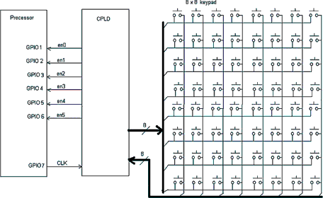
Designers faced with accommodating a keypad requiring more I/O might find that their existing processor (or ASIC) does not have enough GPIO ports. One solution is to use a CPLD as an I/O expander that reduces the I/O requirement of the processor. Figure 2 shows a CPLD interfacing to the keypad rows/columns on one side, and the processor's available GPIO on the other. In this example, an 8 x 8 keypad requires the same number of processor GPIO ports as the 4 x 4 keypad (actually one less) when a CPLD is used. Without a CPLD, the processor would require 16 GPIO ports instead of seven.

Scanning and encoding
Besides reducing the processor's GPIO requirements, the CPLD also scans the rows and monitors the columns for a change in state. When a key is pressed, the CPLD stops scanning and immediately sends an encoded word out to the processor. The encoded word indicates which key was pressed.
In the example shown in Figure 2, there are six bits used to represent the encoded word. Six bits provides 26 or 64 different values each representing a different key. However, one value needs to be used to represent the state when no keys are pressed. Therefore, only 63 keys can be represented in this example. All 64 keys most likely would not be needed in a typical application. If they were, there are many options with a programmable CPLD. For instance, a CPLD could generate an enable signal to the processor that would indicate when a key is being pressed (that is, when the encoded value was valid). This would require one more GPIO on the processor.
The processor is still required to monitor for changes on its GPIO, only, it would not have to deduce which key was pressed since this information is encoded in the six bit word. Debounce will also be required. This can be performed in the CPLD or the processor. Performing this in the processor would keep the size of the CPLD to a minimum.
CPLD design details
Note that the following details describe how the available Verilog reference design is implemented. The concept and design are relatively simple, and additional functionality can be added depending on specific design requirements.
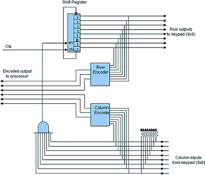
To scan the keypad rows, a barrel shift register is initialised with all ones except for one bit preset to a zero. Each bit of the shift register drives a CPLD output pin that is connected to a row of the keypad. As the shift register is clocked, the zero shifts through the barrel shifter and scans the rows by driving them low one at a time.
The columns are inputs to the CPLD. Each input is pulled up with an internal pull up resistor. When no keys are pushed, all column inputs to the CPLD are passively pulled up to a logic high state. All column inputs are AND'd together. A logic one at the output of the AND gate indicates no keys are pressed. The output of the AND is used as an enable to the shift register.
When a key is pressed, a connection between a row and column is made. The column with the key being pressed will be driven low by the row associated with that key. The output of the AND will go low and disable the shift register for however long the key is pressed.
At this point the shift register is driving the row of the key being pressed to a low, and the column of that key is also at a low. Two encoders are used, one for the row bits (outputs of the shift register), and another for the column inputs. The outputs of the two encoders are grouped together to form the resulting encoded word that is presented to the processor. Figure 3 shows a block diagram of these functions.

Implementation and verification
Xilinx provides a set of application files for CPLD designs free of charge on its website. The reference design is implemented in Verilog [XAPP512 - www.xilinx.com/products/xaw/coolvhdlq.htm] The Xilinx ISE software project is zipped up, including the Verilog source file, Verilog testbench, and UCF file. If you do not have Xilinx software, you can obtain ISE WebPACK for free from the website. WebPACK provides all the tools needed to complete any CPLD project.
The UCF file shows how to initialise the barrel shifter with a pattern of ones and a zero. It also shows how to program the column inputs with internal pull up resistors. The testbench can be evoked from within Project Navigator, which will automatically run a custom ModelSim .do file. The .do file will compile the source code, open a waveform window to view signals, and run the simulation. The testbench generates a clock for stimulus and also simulates the pressing of buttons by periodically connecting a row with a column. This is done until all possible combinations of rows and columns are simulated, and then repeats.
Conclusion
Since the CPLD is reprogrammable, adding a control line, changing the mapping of the encoded word, or accommodating different keypads is possible with the same device. Additionally, other 'glue' functions can be absorbed into the CPLD, such as voltage translators. A specific CPLD device (ie, part number) can be used to accommodate different keypads and even different applications because it is programmable. This helps boost the volume (lowers cost), and reduces risk, since changes can be made even after it is soldered down.
Coolrunner-II also is designed for low power, making it a good choice for battery powered applications, such as cellphones, PDAs, and other portable devices. It also has additional features that augment its low power. Multiple I/O banks can be used for voltage translation, which is another typical application in devices with a mixture of technologies.

© Technews Publishing (Pty) Ltd | All Rights Reserved