22 August 2007Manufacturing / Production Technology, Hardware & Services
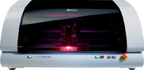
Marantz Business Electronics' M22XDL-650 bench-top automatic optical inspection (AOI) system claims to present today's manufacturers with a breakthrough solution for handling large board sizes of up to 650 mm x 550 mm.
The M22XDL-650 supports comprehensive board inspection, including SMT components, reflow and wave solder joints, and solder paste. In addition, since larger boards typically feature multiple THT connectors, the new machine incorporates unique technologies specifically designed to optimise THT solder joint inspection.
With an inspection capability of 100 000 components per hour, the M22XDL-650 is powered by an Intel Pro Mac control system which equips it to deliver true 24-bit colour imaging. In addition, this product generation introduces an innovative lighting concept incorporating three pulse wave modulated LED light sources and up to six different lighting combinations. When combined with ease of programming and usability, the system significantly enhances operator control for highly reliable board inspection.
Featuring a bottom side clearance of 100 mm and a top side clearance of 40 mm, the M22XDL-650's versatility meets the challenges of odd form components. Since the system's high-speed digital video CCD camera moves in X and Y planes, the stationary PCB can be fixed in place for optimal support, avoiding warping and further enhancing inspection results.
World-first 016008 mm component placement
Manufacturing / Production Technology, Hardware & Services
Fuji has achieved the world’s first placement of 016008 mm (0,16 x 0,08 mm or 006 x 003 inches) size components on printed circuit boards with its SMT pick and place machine, NXTR.
Read more...Lifecycle and obsolescence: Protecting electronics through process Production Logix
Manufacturing / Production Technology, Hardware & Services
At Production Logix, we believe longevity is not accidental. It is engineered through early visibility, structured response, and disciplined execution, in partnership with our OEM customers.
Read more...Maximising squeegee quality and durability Testerion
Manufacturing / Production Technology, Hardware & Services
Transition Automation has announced two new product advancements designed to improve SMT printing performance and extend squeegee life: laser-enhanced Permalex bonding and integrated edge protectors.
Read more...NeoDen ND2 PCB screen printer ZETECH ONE
Manufacturing / Production Technology, Hardware & Services
The NeoDen ND2 PCB screen printing machine is a fully automatic stencil printer designed to deliver precise and consistent solder paste application in modern SMT production environments.
Read more...Understanding the BGA rework process Techmet
Manufacturing / Production Technology, Hardware & Services
BGA rework is a highly technical process that involves removing the faulty component, preparing the circuit board, and installing a new or repaired device, while maintaining the integrity of the printed circuit board.
Read more...Flexible three-process reflow soldering system Truth Electronic Manufacturing
Manufacturing / Production Technology, Hardware & Services
By combining multiple soldering technologies within a single system, the Vision TripleX system enables manufacturers to adapt easily to different assembly requirements, board designs, and production volumes.
Read more...Inline vapour phase soldering for high-volume production MyKay Tronics
Manufacturing / Production Technology, Hardware & Services
The VP2200-100 vacuum inline vapour phase soldering system from ASSCON is designed for fully automated, high-volume electronics manufacturing where process consistency and solder joint quality are critical.
Read more...Global electronics solutions since 1964 IMP Electronics Solutions
Manufacturing / Production Technology, Hardware & Services
Over more than six decades, IMP Electronics Solutions has built a reputation for technical expertise, reliable supply chains, and strong partnerships with both customers and manufacturing partners.
Read more...Driving excellence in electronics manufacturing Jemstech
Editor's Choice Manufacturing / Production Technology, Hardware & Services
Jemstech’s reputation for disciplined execution and client-focused service has earned it strong loyalty from companies operating in demanding industries.
Read more...When do you need Nitrogen in reflow? Truth Electronic Manufacturing
Manufacturing / Production Technology, Hardware & Services
Nitrogen in reflow soldering is often seen as a performance enhancer, offering improved wetting, shinier joints, and fewer defects. But it is not always necessary.
While every effort has been made to ensure the accuracy of the information contained herein, the publisher and its agents cannot be held responsible for any errors contained, or any loss incurred as a result. Articles published do not necessarily reflect the views of the publishers. The editor reserves the right to alter or cut copy. Articles submitted are deemed to have been cleared for publication. Advertisements and company contact details are published as provided by the advertiser. Technews Publishing (Pty) Ltd cannot be held responsible for the accuracy or veracity of supplied material.


 printer friendly version