


From the early days, the mantra for the semiconductor industry has been ‘smaller, better, faster and cheaper’.
The current Pocket PCs are more powerful than the first computer, which required a separate building.
The way this goal has been achieved, so far, is to reduce the size of the individual transistors used to create the semiconductor devices. This has an interesting side effect. As the transistor gets smaller, the operating voltage gets lower. The 5 V power-supply rail used to be the most popular rail in embedded systems. However, most components in typical embedded systems are moving toward lower rails to take advantage of the latest trends in the industry.
On the other hand, some components in the system take longer than others to transition. Therefore, in this transition phase it is possible that some components in the system may require different power-supply rails (ie a 5 V device in a 3,3 V system, and vice versa). This creates some design challenges for an embedded designer. One solution is to use level translators. However, the use of a level translator is not the most cost-efficient solution. This article discusses a few low-cost ideas to interface a 3,3 V microcontroller (MCU) to a 5 V peripheral.
When moving a 5 V design to 3,3 V, the first thing to consider is a 3,3 V version of the same device. In most cases, there will be an equivalent device supporting the 3,3 V rail. Most of the time, 3,3 V devices are available at either the same cost or cheaper. If an alternate device that runs at 3,3 V is not available, then using two rails may be the answer. The main focus of this article is on designs that use two voltage rails.
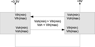
When bringing two people from different worlds together, it is important to ensure that they can understand each other. The same is true when bringing the 5 V world and the 3,3 V world together. First comes an understanding of the voltage logic levels and input/output structure. For inputs, consider the voltage that is warranted to be detected as high input (VIH) and the voltage that is warranted to be detected as low input (VIL). When interfacing a 3,3 V system to a 5 V device, the VIH tends to be a bigger problem than the VIL. However, it does not mean that the VIL spec can be ignored. The driving devices must output a voltage higher than the VIH(min) spec of the receiving device to ensure proper logic detection. Too high a voltage may also cause problems.
Almost all CMOS devices have some kind of electro-static discharge (ESD) protection on all I/O pins. The most common way to implement this protection is to have a clamping diode to Vdd and Vss. Generally, this translates into a maximum input voltage spec of Vdd + 0,3 V and a minimum voltage spec of Vss - 0,3 V. If this spec is exceeded, then protection diodes may start conducting. If the input does not have a series resistor, then it may result in very high current through these diodes, potentially causing latch-up; not a desirable condition.
If the voltage is roughly high enough (ie 5 V input in a 3,3 V system), then the series resistor needs to be very high to reduce clamp current to a safe range. If the resistor is high enough, then the low-input capacitance due to pin capacitance and PCB layout may be significant and the RC time constant causes signal delay. Many manufacturers do not recommend the use of an ESD protection diode as a clamp diode, therefore, the use of a series resistor is not the best option to feed a 5 V signal to a 3,3 V device.
When considering the logic levels of a standard CMOS device, most tend to have VIH (min) of 0,7 Vdd or 0,8 Vdd. The VIL(max) tends to be in the region of 0,2 Vdd or 0,3 Vdd. For 5 V logic, this translates into VIH of 3,5 V or 4,0 V and VIL(max) of 1,0 V or 1,5 V. Most CMOS devices output close to rail (0,1 or 0,2 V drop) at a lower load. As the load current increases, VOH tends to be lower. In this scenario, the load current must be considered in order to determine VOH.
Instead of an input series resistor, a better option is to use a resistor divider to bring the 5 V signal in range for 3,3 V input (see Figure 2). The resistor value should be selected in such a way that it accounts for all the tolerances. The following formulae assist in the calculation:
R2/(R1 + R2) * VOH(min) @ min of 5 V (at maximum negative tolerance) > VIH(min)
R2/(R1 + R2) * VOH(max) @ max of 5 V (at maximum positive tolerance) < VIH(max)
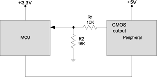
Resistor tolerance should also be a consideration in the above calculations.
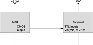
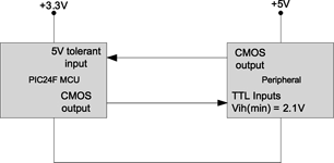
Another, simpler solution is to use a 5 V device with TTL inputs. The VIH(min) for a TTL device is 2,1 V (for a Vdd of 5 V). Most of the 3,3 V devices can support a much higher VOH level at a high load rate. In this case, the solution is to replace the peripheral device with an equivalent device having TTL-compatible inputs.
If using a standard digital logic family that must run at 5 V, then equivalent devices with TTL inputs should be available. For example, the 74HCT family can be used to replace 74HC series devices. If a level translator is needed, then HCT or VHCT digital buffers can be used. In most situations, this TTL-input solution tends to be cheaper than the use of dedicated level translators.
The VOH level of the device operating at 3,3 V is slightly below the VIH (0,7 Vdd = 3,5 V) of the CMOS device operating at 5 V. One simple solution is to use a diode to provide the required voltage shift.
The circuit shown in Figure 4 shifts the output by approximately 0,6 V on the positive side. This shift of 0,6 V to CMOS output brings it in range for 5 V CMOS input. The same amount of shift is applied to the logic low signal. However, VIL (max) for the CMOS input tends to be around 1,5 V, so the shifted signal will not violate the VIL spec.

There are however several factors to be considered in this configuration. When the 3,3 V device outputs a zero logic level, it increases the current draw. Examine the VOL spec of the 3,3 V device for this current sink. Typically, the higher the sink current, the higher the VIL. Here, care should be taken to avoid violating the VIL spec. If the CMOS output VOL is higher, then increasing the pull-up resistor value can be considered. If the resistor value is too high, then the diode bias current will be low and the diode may not be able to switch fast.
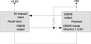
Devices such as Microchip's PIC24 family of 16-bit MCUs offer one unique feature to simplify the 5 V interface. They offer 5 V (or 5,5 V) tolerant inputs, even if the device runs at a Vdd of 3,3 V or lower. They do not have a clamp diode to the Vdd and use a different type of ESD protection mechanism to support this capability. This is a very important feature for the 5 V interface, as it allows a 5 V output to be connected directly to a 3,3 V device without a resistor divider. The example in Figure 5 shows that this feature allows for a seamless 5 V interface.
Some MCUs further enhance this feature by providing the option to generate a 5 V output with an external 5 V pull-up resistor. The 3,3 V device drives a 3,3 V output, but it can tolerate a 5 V input. The digitally-controlled open-drain output capability on these pins allows them to be pulled up to 5 V without violating any specs. This feature supports a simple interface to 5 V devices with CMOS inputs.
When using the pull-up resistor configuration shown in Figure 6, the capacitance of the connection between the two devices needs to be considered to determine the rise/fall rate (as does the maximum switching frequency) of the signal on this port pin, and the resistor value that is appropriate for the application. Consider the following equation:
Where τ = RC time constant, R*C
PVdd = Vdd of the peripheral voltage
PVIH(min) = The VIH(min) value of the peripheral
Using the following typical values:
Pull up resistor R = 1 kΩ
Resultant capacitance C due to pin and PCB capacitance ≈ 10 pF
PVdd ≈ 5 V
PVIH (min) ≈ 0,7 * Vdd ≈ 3,5 V
The resultant rise/ fall time ≈ 12 ns
If the minimum acceptable pulse width for this rise/fall time is 50 ns, then it results in a maximum output frequency of 20 MHz. This is sufficient for most peripheral interactions.
This configuration has one side effect when the MCU drives the logic low; the extra current is burned through a pull-up resistor. The pull-up resistor offers design trade-offs for speed against current draw. It may be necessary to select a compromise value for the application that provides the required speed and current consumption for the application.
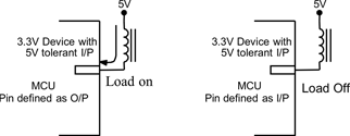
Some may say that this kind of configuration can not be used to drive a low-impedance load. So what are the options for driving a 5 V relay? Fortunately, the above feature is also helpful for driving low-impedance loads like relays. Figure 7 shows the relevant circuit configuration. To drive the load, define the pin as an output and drive it low. The only limiting factor here is the current-sinking capability of the device. To turn off the load, define the pin as an input. This will turn the load off and will result in 5 V at input. The pin is 5 V tolerant, so this is a valid operation. In other words, it is necessary to maintain logic low on output latch and toggle input/output control register to turn the load on/off.
This is an effective way to bridge the 5 V and 3,3 V rails. It is possible to devise similar low-cost, intelligent solutions to bridge two rails during the transition phase.
| Tel: | +27 11 608 0070 |
| Email: | [email protected] |
| www: | www.cstelectronics.co.za |
| Articles: | More information and articles about CST Electronics |
| Tel: | +27 11 458 9000 |
| Email: | [email protected] |
| www: | www.electrocomp.co.za |
| Articles: | More information and articles about Electrocomp |
| Tel: | +27 11 923 9600 |
| Email: | [email protected] |
| www: | www.altronarrow.com |
| Articles: | More information and articles about Altron Arrow |
| Email: | [email protected] |
| www: | |
| Articles: | More information and articles about Tempe Technologies |


© Technews Publishing (Pty) Ltd | All Rights Reserved
 printer friendly version