


Low-cost ASK and/or FSK transmitter and transceiver ICs are key components in short-range radio systems designed to work in unlicensed industrial, scientific, and medical (ISM) bands between 300 MHz and 450 MHz. Applications for these short-range devices (SRDs) include remote keyless entry (RKE), tyre-pressure monitoring (TPM), remote-control and security systems.
System design, which addresses RF link budgeting, antenna design, battery life, and regulatory concerns, among a multitude of other issues, often involves a trade-off between the output power and the current drain of the transmitter. The power amplifier (PA) on Maxim's low-cost transmitters and transceivers (such as the MAX1472, MAX7044, MAX1479, and MAX7030/MAX7031/MAX7032) possess an unique feature that allows the user to control the RF power-/current-drain tradeoff while maintaining high efficiency. Managing that trade-off is key to maximising battery life for a particular application. The Maxim ICs require no modifications to handle this trade-off; simply changing the load impedance presented to the PA can change the PA's output power and current drain.
This article by Maxim's Andy Zocher briefly overviews power amplifier theory and then presents simulation results for insight into the operation of the PA on all Maxim LFRF transmitters and transceivers.
Power amplifier overview
Class A, B, and C amplifiers
A Class A amplifier is characterised by a combination of bias point and signal level where the device's average current drain does not change with the magnitude of the input signal. In Figure 1, M1 can be assumed to be a current source of magnitude IDC.
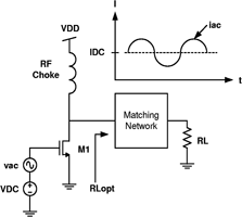
It is well known that the impedance for maximum output power is:
RLopt = VDD/IDC
The maximum output power is defined as:
Poutmax = 0,5 ∞ VDD ∞ IDC
Therefore, the peak efficiency is 50%[1]. This analysis assumes that the drain voltage of M1 can swing to ground while still maintaining a bias current of IDC. Operation in the triode region limits the practical efficiency of Class A CMOS PAs to less than 40%. As this analysis implies, the bias current of a Class A amplifier must be changed to maintain a reasonably high efficiency for different output-power levels for a given supply voltage. Class A amplifiers are most amenable to modulation schemes where linear amplification of the input signal is important, since the bias point does not change with the magnitude of the input signal.
Class B and Class C amplifiers, however, offer higher efficiencies than the Class A amplifier, but usually at reduced output-power levels and with more distortion.
The common characteristic of all Class A, B, and C CMOS amplifiers is that the active device is considered to be a voltage-controlled current source and operation in the triode region is undesirable.
Class D, E, and F amplifiers
In contrast to Class A, B and C amplifiers where operation in the triode region should be avoided, the Class D, E, and F CMOS amplifiers rely on operation in the triode region for optimum efficiency and output power. These amplifiers are often called 'switching-mode' amplifiers and are typically used in ISM-band transmitters and transceivers because of their inherent high-efficiency operation at low voltages. In a switching-mode amplifier, the output device is driven by a large-signal square wave, as shown in Figure 2.
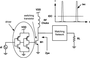
Think of the output transistor as a resistor that is switched on and off at the operating frequency with a given duty cycle. As Figure 2 indicates, the current in the output device can be very rich in harmonics. This harmonic content depends on the duty cycle and magnitude of the driving waveform, the FET 'on' resistance, and the impedance presented to the PA. In a Class D amplifier, the duty cycle of the input signal is varied to control the output power, a process known as pulse-width modulation (PWM). Class D amplifiers are utilised most often in audio applications where the power delivered by the amplifier changes constantly.
In a Class E amplifier, the duty cycle of the input signal is fixed. The matching network is designed to minimise the voltage at the drain terminal of the switching while the switch is on. By minimising the voltage across the output device while the output device draws current, one can minimise the power dissipated by the switching device and, therefore, maximise PA efficiency.
Similar to a Class E amplifier, a Class F amplifier requires special attention to the harmonic impedances in the design of the matching network in order to enhance efficiency. In general, the matching circuits for Class F amplifiers are more complex because of the design constraints placed on harmonic impedances.
Switching-mode amplifiers
All Maxim CMOS ISM transmitters and transceivers provide an open-drain PA output. The duty cycle of the driving signal is a constant 25% over the full range of 300 MHz to 450 MHz. The user will design the matching network that provides the desired output-power level, current drain, and harmonic performance.
A simple model for a switching mode PA output is illustrated in Figure 3.
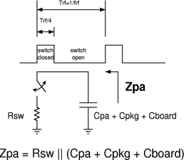
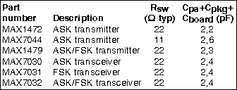
In this illustration, Rsw is the on-resistance of the FET, Cpa is the effective sum of the device parasitic capacitances, Cpkg is the package capacitance, and Cboard is the board capacitance. Table 1 summarises the typical switch resistance and capacitance for the Maxim ISM transmitters and transceivers.
Note that the typical switch resistances are given for VDD = 2,7 V and that the board parasitic capacitance can vary significantly with layout. Class E and F amplifier theory and matching network-design equations are well documented in literature[2,3,4] and the reader can refer to these for additional guidance. Considering the scope of this application note, it is sufficient to say, firstly, that the matching network and, therefore, the waveform at the PA output node must be designed to maximise the PA efficiency. Secondly, the maximum efficiency occurs when the voltage across the device is low when the switch is closed.
Switching-mode amplifier simulations
In many low-cost ISM applications, the system designer may not have much flexibility in design time, cost, or complexity to optimise the PA matching network for maximum efficiency. Small (high-Q), inexpensive antennas are generally more efficient at transmitting higher frequencies, but regulatory concerns limit the harmonic content of the transmitted signal. Therefore, harmonic attenuation by the matching network is extremely important. Considering these facts, we analysed the switching PA with the assumption that the output-matching network will be designed so that the voltage at the drain is highly filtered and therefore sinusoidal. See Figure 4.
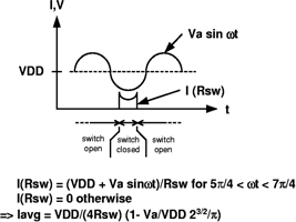
Assuming that the PA is loaded with a resistance of RL and that the output voltage can swing as low as 0,1 V, the efficiency of the PA can be expressed as:
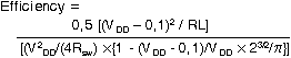
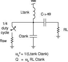
If VDD = 3 V, Rsw = 22 Ω and RL = 400 Ω, then the PA efficiency is 80% with an output power of 10,2 dBm. Of course, the voltage waveform, the switch resistance, and the load impedance are interdependent, so the above equation cannot be used as an accurate predictor of efficiency for all combinations of the variables. For this reason, SPICE has been used to model the performance of an ideal switching-mode PA. An ideal switched resistance of 11 or 22 Ω is placed across a parallel tank circuit with a Q of 10. The simulation schematic is illustrated in Figure 5; the simulated results are shown in Figure 6.
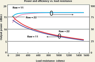
As Figure 6 indicates, one of the most significant advantages of the switching-mode PA is that the output power can be varied over a wide range by changing the load presented to the PA while excellent DC-to-RF efficiency is maintained. In addition, a switching amplifier with a lower switching resistance can put out more power at a higher efficiency, when compared to a higher switching resistance. The drawback of a lower switching resistance is that a higher driver current is required to charge and discharge the parasitic capacitance of the switching device.
To maximise the efficiency of a switching-mode amplifier, the switch must be turned on only near a minimum in the voltage waveform. For the example of the switched resistor loaded with a simple parallel resonant circuit, one can satisfy this requirement by minimising the imaginary component of the impedance presented to the PA at the operating frequency (including the parasitic capacitances of the device, package, and board). If the network is off resonance, or detuned, the efficiency can degrade significantly. Figure 7 illustrates the performance of an ideal switching-mode amplifier if the matching network is off resonance for Q=10 and Q=5.
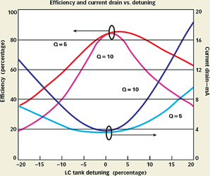
As seen in Figure 7, a current-drain minimum occurs at resonance. This fact can be used to verify that a given network has been optimised for a particular operating frequency. It should also be noted that the SPICE simulations assume that: the switch resistor can be turned on and off instantly; the parasitic capacitance of the switched device does not change as the device is turned on and off; and there is no loss or parasitic impedances in the tank inductor or capacitor. These factors can degrade the performance of an actual switched-mode amplifier when compared to the ideal simulations. An iterative approach is often required to optimise the PA matching network for a particular application.
References
[1] Behzad Razavi, RF Microelectronics, Prentice Hall, Engelwood Cliffs, NJ, 1997.
[2] N.O. Sokal and A.D. Sokal, 'Class E: A New Class of High Efficiency Tuned Single-Ended Switching Power Amplifiers', IEEE J. Solid-State Circuits, vol. SC-10, pp. 168-176, June 1975.
[3] Scott Kee, Ichiro Aoki, Ali Hajimiri, and David Rutledge, 'The Class E/E Family of ZVS Switching Amplifiers', IEEE Transactions on Microwave Theory and Techniques, MTT-Vol.51, No. 6, May, 2003.
[4] High-Efficiency Class-E Power Amplifiers, Part I & II, Eileen Lau, Kai-Wai Chiu, Jeff Qin, John Davis, Kent Potter and David B. Rutledge, QST, Journal of the American Radio Relay League, May & June 1997.
| Tel: | +27 11 608 0070 |
| Email: | [email protected] |
| www: | www.cstelectronics.co.za |
| Articles: | More information and articles about CST Electronics |
| Tel: | +27 11 458 9000 |
| Email: | [email protected] |
| www: | www.electrocomp.co.za |
| Articles: | More information and articles about Electrocomp |


© Technews Publishing (Pty) Ltd | All Rights Reserved
 printer friendly version