


The PADS Router from Mentor Graphics is an advanced, interactive trace editor that is available to printed circuit board designers as part of the PADS product flow of electronic engineering software design tools.
The PADS Router utilises Latium technology to deliver efficient initial and post trace modification capabilities.
Interactive routing
Most routing solutions today consist of one of two methodologies – manual routing and automatic routing.
Manual routing means each trace is placed by ‘tracing’ the exact pathway defined by the mouse cursor; every corner is defined usually by clicking the mouse and the system flags design rule clearance violations via a graphic indication.
Autorouting is just the opposite, where design rules are defined and the design is submitted to the system which proceeds to route without interaction; results are then reviewed post route.
Interactive routing is a technique that gives the designer the control of manual routing, but with the speed of autorouting. The PADS Router is an interactive routing environment which utilises a ‘push-n-shove’ methodology to allow seamless initial trace placement and post trace modifications.
Traces and vias placed on a printed circuit board (PCB) design dynamically shift their locations as new traces and vias are introduced into an area, allowing the designer to review an area before deciding to commit to a particular pattern. The PADS Router recognises and utilises the PADS Layout constraint hierarchical structure to ensure the proper constraint definitions are maintained during trace placement.
Users can easily change layers while the router maintains the proper spacing on all items, on all layers, in realtime. Via definition can also be incorporated as part of the required constraints, so that only particular vias are inserted as the trace bridges multiple layers.
The PADS router also manages high speed constraints associated with minimum and maximum length, and matched lengths. Constraints can be specified in both the schematic capture and layout programs, and the router responds with the same realtime feedback behaviour.
Signals requiring special coupling can have constraints set and maintained automatically while the trace is placed in the design. Adjacent traces maintain the proper clearance while the coupled traces are placed, resulting in minimal resistance throughout the entire trace addition process.
Trace addition
Users can begin trace additions by selecting the appropriate tool in the software. This places the software in a verb/object mode that allows an action to be applied to any object selected. This provides users with a single selection route mode, so traces can be placed quickly, one after another.
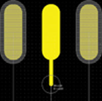
Once in this mode users select either a device pad or an unrouted connection. By selecting the device pad, a trace is generated immediately with the proper width extending from the selected device pad (Figure 1). As the cursor is dragged through the design, the PADS Router dynamically clears obstacles directly in the path of the trace being placed.
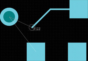
If users choose to select an unrouted connection, the PADS Router may start on either side of the pin-pair depending on how close the cursor is to either pad. The PADS Router attempts to auto-connect the trace being placed to the pad nearest to the cursor when selected (Figure 2).
Pin pair orders can be modified ‘on the fly’ while placing traces, giving users maximum routing flexibility. On nets that require specific routing requirements, there are routing controls that provide restrictions on inter-connecting pads, so a specific order is maintained. There are even special modes, such as Mid-Driven, Serial Source and Parallel Source, that can be enabled to produce special routing patterns depending on the net geometry requirements.
As traces are placed in the design (Figure 3), regardless of the defined net constraints, the PADS Router has multiple choices as to how it handles those obstacles, including:
* Routing over obstacles with trace segments automatically removed.
* Having violating obstacle locations adjusted to compensate for the additional traces.
* Having DRC set to inform the user any time they place traces too close to other items whose constraints have not been maintained.
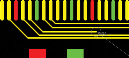
Having multiple choices in trace placement adds to the flexibility that makes the PADS Router engine highly efficient.
Trace modifications
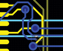
The PADS Router not only allows initial trace placement but it also allows trace modification (Figure 4). Trace data can be completely rerouted while still utilising the PADS Router’s power to push-n-shove placed obstacles completely out of the way. Users simply select the trace segment they wish to begin the modification at, place the new desired trace segments and then reconnect back into the existing trace to complete the modifications. All the while the PADS Router is reviewing the trace constraints to ensure that all modifications still conform.
The PADS Router can shove not only individual trace/via obstacles but multiples as well (Figure 5). If a trace needs to be adjusted in an area where an entire bus exists, the user simply selects the trace and stretches it to the desired location. Any adjacent traces will automatically adjust to accommodate the new location. If 45° corners were utilised in the trace being moved, all the associated 45° traces will be maintained after the adjustment as well. If vias need adjusting, users simply select the desired via and drag it to a new location with traces automatically adjusting to the new location.

Conclusion
PCB design layouts, whether simple or dense, can benefit from the PADS Router’s power, and intuitive methodology. As design constraints become more prevalent in everyday designs, PCB designers can no longer keep track of every net, class or length based rule during trace placement. The PADS Router overcomes these obstacles, allowing the circuit board designer to focus on resolving other more complex design issues.
For more information contact ASIC Design Services, +27 (0)11 315 8316, [email protected], www.asic.co.za
| Tel: | +27 11 315 8316 |
| Email: | [email protected] |
| www: | www.asic.co.za |
| Articles: | More information and articles about ASIC Design Services |


© Technews Publishing (Pty) Ltd | All Rights Reserved
 printer friendly version