


As we all know, the process geometries of both digital and analog integrated circuits are continually shrinking - with the clear advantages of lower power requirements, silicon areas and prices.
However, this reduction in geometry size does have implications for board designs. A simple substitution of a device manufactured with a 0,25 μm (micron) process in place of one manufactured in a 0,7 μm process can produce unexpected results.
Why is this? In theory, nothing has changed, but the evidence contradicts this. One option is to avoid using smaller-geometry devices, but this is very short-sighted. Such a decision means that systems will not benefit from lower power-supply voltages, faster speeds and lower cost - making them uncompetitive in a very short time.
The best approach is to design in the expectation that geometries will continue to shrink. An important issue to consider is increased susceptibility to electrostatic discharge (ESD). Smaller-geometry devices are less able to absorb high-voltage transients and lack robustness around high currents. The manufacturers' standards are not reduced, with a 2000 V r.m.s. to 4000 V r.m.s. ESD tolerance (Human Body Model). However, their tests look for catastrophic failures while the end-user can experience RAM contamination caused by electromagnetic interference (EMI) or electrical fast transient (EFT) signals.
A number of approaches can help with this problem, including protection circuits (MOVs, transient suppressors), microcontroller or processor pin protection (I/O, interrupt, reset pins), or firmware recovery techniques (WDT, register refresh), etc. All of these techniques help to produce a more-robust design, but the most significant results are achieved by layout optimisation.
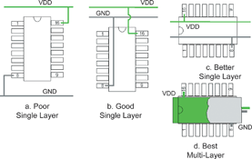
To move to smaller-geometry devices, it is important to look at places on the board layout where spikes and glitches can enter the newly-sensitive circuits. One of the most productive places to look, is at the power-supply tracks. In a typical circuit, buck- or boost-converters provide the power supplies. This type of supply is inherently noisy, but there is also the risk of added EFT signals, in the form of voltage or current spikes. These may be quite acceptable in circuits using larger-geometry devices, but can cause problems as smaller geometries are used. A general rule-of-thumb is to minimise these effects by managing the power and ground traces (or planes). Finally, the circuit has always required decoupling or bypass capacitors, but now, accurate selection is critical. Figure 1 illustrates a range of techniques that offer different levels of effectiveness.
Summary
Of course, these are not new suggestions, but many engineers have discovered that not all of them have to be implemented too carefully for circuits using larger-geometry devices. Now, the situation is changing. As new silicon geometries work their way into designs, board layouts must be optimised with power glitches in mind: add protection circuits such as MOVs and transient suppressors; protect the I/O, interrupt and reset pins of the controller or processor; use firmware recovery techniques such as WDT or 'register refresh' so that they contain the correct values. All of these techniques will help to produce a robust design.
| Email: | [email protected] |
| www: | |
| Articles: | More information and articles about Tempe Technologies |
| Tel: | +27 11 923 9600 |
| Email: | [email protected] |
| www: | www.altronarrow.com |
| Articles: | More information and articles about Altron Arrow |


© Technews Publishing (Pty) Ltd | All Rights Reserved
 printer friendly version