


Differential signalling (DS) is defined as a digital signal that is transmitted on a two-wire system where complementary voltage levels exist on the two wires. DS is one of the hottest topics in high-speed digital design because more and more designs are running in the GHz frequency range and edge rates are in the sub-nanoseconds.
When transmitting data on high-speed buses over long haul transmission lines, using single-ended transmission is virtually impossible due to losses (Cu, skin effect and dielectric), jitter and an increase in bit error rate (BER). Therefore, DS is being used not only for cable transmission but also for large backplanes, mother/daughter PCBs and buses like PCI and XAUI.
A real-world example of high-speed DS is at Intel. Here a 4 GHz clock was transmitted on a cable. 70% of the signal was lost due to Cu, skin effect and dielectric. Even though the received amplitude was only 30% of the transmitted amplitude, Intel did not have one BER fault. Obviously if this were a single-ended transmission, the receiver would not be able to distinguish the one/zero data stream.
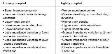
When DS is being considered, one of the first design considerations is to determine if they should be loosely coupled or tightly coupled. Table 1 provides a summary of pros/cons of each design concept.
Let us look at each of these elements in a bit more detail:
1. Impedance control
With loosely coupled, the microstrip width (w) to height (h) ratio can be more closely controlled (for FR4 material with DR = 4,5, to obtain 50 Ω, w = 1,6 x h).
2. Sensitivity to manufacturing variations
The wider the trace, the less variation in Z0 with respect to manufacturing tolerance. The biggest tolerance factor is the Cu etching process and for wide traces, ie, 10 x 10 mil, the Z0 tolerance should less than 5%.
3. Track density
With loosely coupled, the lower track density equates to less routing on each layer, therefore on a dense PCB there are more layers and typically more cost. This is especially true for a PCB with BGAs that are fully populated, ie, balls covering the entire mounting area.
4. Even mode return loss
This is the same as common mode reflection, due to driver skew, metastability and different trace lengths. Matching lengths is easier with loosely coupled since they are more manoeuvrable.
5. Insertion loss
This is DC conductor loss, AC conductor loss and skin effect. It is obvious that there is less DC and AC conductor loss with larger traces, ie, more Cu = less resistance. Skin effect is a function of the square root of frequency in the numerator and perimeter in the denominator. Therefore, the larger the trace, the lower the skin effect losses.
6. Impedance variation at 2 mm connector transitions
There will be less reflection with 10 mil to 80 mil traces than if the trace is 5 mil. Design guides can be followed for connecting any discontinuity and eliminating mismatch reflection.
7. Impedance variation at BGA escape transitions
Typical BGA pad spacing is 25 mil. Therefore, a 50 mil pitch (1,27 mm) results in 0,68 mm spacing. If routing is 3 x 4 mil, then three channels can be routed in 25 mil which is the typical space between BGA pads. If routing is 5 x 5 mil, then only two channels can be routed.
8. Impedance variation at via transitions
If the trace impedance Z0 and via impedance ZV are unmatched, the easiest method to make them equal is changing the pad diameter. If this increases then C increases and ZV will decrease. The larger the trace width, the easier it is to match Z0 with ZV.
9. EMI
This is a major consideration. Refer to Figure 1. Odd mode means there are equal and opposite voltages on each conductor. For example, on the left conductor a positive (+2 V) signal exists, and on the right conductor a negative (-2 V) signal exists. Hence, per the right-hand rule, equal and opposite magnetic fields will exist around the conductors as shown.
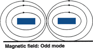
The more tightly the traces are laid out, the more the magnetic fields cancel each other, and the more tightly they circulate around their respective conductor. This in turn minimises radiated emissions.
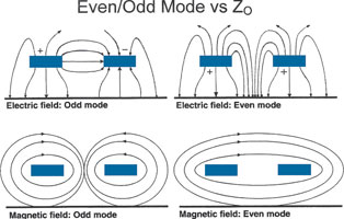
In Figure 2a, odd (differential) and even (common) propagation modes are illustrated. The differential mode (DM) is what the designer wants on the pair, ie, equal and opposite voltages. Due to driver skew, metastability and different trace lengths, an even common mode (CM) voltage can also occur, which is an undesirable condition.
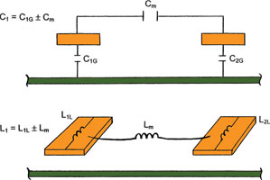
In Figure 2b, the actual capacitance and inductance that are associated with either trace, and the effect of coupling to the matching differential trace are shown.
In Figure 2c, the effects of the DM and CM coupling can be defined. For DM (odd), as the traces become more tightly coupled, the impedance decreases. For CM (even) just the opposite will occur. As the impedance decreases, the width of the trace must decrease at the same ratio. This will keep Z0 at a constant value. For CM, the way to minimise its effect is with proper termination at the receiver. Regarding whether propagation delay increases or decreases will depend on the ratio of the changes in L1L and C1G.
Summary
As each new design evolves, there will be an ever increasing need for differential signalling. This is mandated by the requirement to outdo or keep pace with the competition. Also, with the die shrink that is occurring in all ICs, edge rates are becoming steeper. These two factors require better control over ground bounce, transmission line reflection, crosstalk, bypassing/power delivery and radiated emissions. The best way to control these unwanted high-speed phenomena is the proper use of differential signalling.
All the topics discussed in this article will be presented during the High-speed Digital Design Seminar, scheduled for 11-13 May at the Innovation Hub in Pretoria.
| Tel: | +27 12 665 0375 |
| Email: | [email protected] |
| www: | www.edatech.co.za |
| Articles: | More information and articles about EDA Technologies |


© Technews Publishing (Pty) Ltd | All Rights Reserved
 printer friendly version