


The nRF series of single-chip radios from Nordic is an easy way to get into the expanding market of short-range wireless communications. A printed circuit board (PCB) with one of these chips, together with a suitable microcontroller and an antenna is essentially all that is needed to build up a wireless communication link.
However, there are some guidelines that need to be followed to end up with an optimal solution. In this article Nordic gives a brief look into common problems that may occur. Special focus is set on the problems related to integrating digital circuitry and an RF chip on the same board, followed by some advice to solve these problems.
Why are digital and analog circuits potential enemies?
Analog (radio) and digital (microcontroller) circuitry might work well for themselves, but once put on the same circuit board and the same power supply, things can get a little more complicated. Digital signal lines most often swing between ground and positive power supply, which for most applications means a peak to peak amplitude of ~3 V. Switching time of digital signals is fast, normally in the nanosecond range. Due to the large amplitude and fast switching, the signal will contain a considerable amount of high frequency components, independent of the switching frequency. On the analog side, the input signal from the antenna to a radio receiver can be less than 1 μV rms. The magnitude difference between the digital and RF signal can therefore be as large as 1 million (120 dB). It is evident that if these signals are not separated or shielded properly, the weak RF signal may be corrupted, with radio performance deterioration or even malfunction as a result.
Common errors combining RF and digital on one PCB
Insufficient separation between sensitive and noisy signal lines: As mentioned, digital signals have high amplitudes and contain high-frequency harmonic components. High frequency signals can couple between adjacent lines on the PCB if such a signal is routed adjacent to a sensitive analog signal. The most sensitive nodes on RF devices are normally the loop filter of a phase locked loop (PLL), the external inductor of a voltage controlled oscillator (VCO), crystal reference signals and also, of course, the antenna terminals. These parts of the circuit should be handled with special caution.
Power supply noise: Because digital devices operate with input/output signals with several volts in amplitude, they are generally robust to power supply noise. On the other hand, analog circuits can be extremely sensitive to power supply noise, especially spikes and other high frequency components. Therefore the power supply routing on PCBs containing RF (or other analog) circuitry must be done with much more caution than on a plain digital board. Auto routing should be avoided.
It is also important to note that microcontrollers (or other digital circuitry) tend to draw most of the current in short bursts at each internal clock cycle. This is due to the fact that modern micros are all designed in CMOS. Thus, if a microcontroller is running at an internal clock frequency of 1 MHz, it will draw current pulses from the power supply at this frequency. Inevitably, this leads to voltage spikes on the power supply line if proper de-coupling of the power supply is omitted. If these spikes reach the power pins of the RF part of the circuitry, serious malfunction might result. It is therefore mandatory to keep separate power lines to the analog and the digital domains of the circuit (star routing of VDD).
Grounding an RF system: RF circuit boards should always be laid out with a ground plane connected to the negative power supply. If this is not done properly, obscure circuit behaviour might occur. From a digital designer point of view, the reason for this might be difficult to understand, as most digital circuitry functions very well without a ground plane. At RF frequencies even a short line will work as an inductor. As a coarse rule of thumb, the inductance will be about 1 nanohenry per mm of length. At 434 MHz a 10 mm PCB line will then present an inductive impedance of 27 Ω. If a ground plane is not used, most ground lines will be longer than this and the RF circuit board will almost be guaranteed not to function.
Radiation from antenna to other analog parts: Electromagnetic field radiation is often overlooked in circuits containing radio and other circuits. The board often includes other analog circuitry than the RF part. For instance, many microcontrollers contain built-in analog-to-digital converters (ADCs) that can be used to measure analog inputs, battery voltage or other parameters. If the antenna of a radio transmitter is located near the PCB (or even on the PCB), the transmitted high-frequency signal might reach the analog input of the ADC.
Remember that any piece of circuit board line can function as an antenna for emission or reception of RF signals. If the ADC input has insufficient termination, then the RF signal may be rectified in the ESD diodes at the ADC input, and this can result in an offset in the ADC.
Some practical hints that really make things work
Below are given a few general design and layout tricks that can be used in most RF applications. However, it is important that layout advice for the actual RF component should also be followed.
The RF designer's best trick: A solid ground plane should always be used when designing a PCB containing RF components. The purpose is to create an efficient 0 V-reference node in the circuit that everything can be de-coupled to. The 0 V terminal of the power supply should be coupled directly to this. Due to the low impedance of the ground plane, there will be no signal coupling between two nodes that are de-coupled to it. This is very important, as there are signals on the board with a difference in amplitude as large as 120 dB.
With surface mounted PCBs, all signal routing is done on the same side as where the components are mounted, and the ground plane will be on the opposite side. Preferably the ground plane should cover the complete PCB (except under PCB antennas). If a PCB with more than two layers is used, the ground plane should be placed in the layer that is adjacent to the upper signal layer (ie, layer no. 2 counted from the component side).
It is also a good idea to fill all available space at the signal routing layers with ground planes. These ground planes must then be connected to the main ground plane with multiple vias. Please note that the characteristics of inductors will be changed by the presence of a ground node close by. This must be taken into consideration when selecting value and placing of these.
Short connections to ground plane: All connections to the ground plane must be made as short as possible. A via should be placed close to every pad that is to be grounded. Never let two ground pads share one via, this can lead to crosstalk between the two pads due to the impedance of the via itself.
RF de-coupling: De-coupling capacitors should be placed as close as possible to the pins that are to be de-coupled. Use one de-coupling capacitor for each node that is to be de-coupled. Use high quality ceramic capacitors, preferably of the 'NP0' dielectric type but 'X7R' will work well for lower frequencies. The value of the capacitors should be chosen so that their series resonance frequency is equal to the signal frequency they are to de-couple.
For instance at 434 MHz, a 220 pF NP0 SMD-mounted 0603 capacitor will give the best de-coupling. The series connection of the impedance in the capacitor and the via creates a 'notch' filter at the signal frequency, which gives a very efficient decoupling. At 868 MHz a 33 pF capacitor gives the same effect. In addition to the small value RF de-coupling, a high value capacitor should be placed at the feed line from the power supply to de-couple low frequencies as well. A 2,2 μF ceramic or 10 μF tantalum would be a good choice for this.
Star routing of power: Star routing (Figure 1) is a well-known layout trick in analog design. Separate power lines for each module are routed directly from the power supply. These power lines should be de-coupled separately, close to the IC packages in addition to the star node de-coupling.
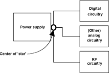
This is an efficient way of isolating power noise from the digital part from reaching the RF part. If extremely noisy modules are placed on the same circuit board, inductors or low value resistors (10 Ω) may be placed in series with the power supply line to these modules. Tantalum capacitors of at least 10 μF must be used to decouple the power supply at these modules. Examples of such modules are RS232 drivers or switched-power regulators.
Floor planning of PCB: To reduce the risk that noisy modules disturb the analog part, the location of the modules on the circuit board is essential. Always locate sensitive modules (RF part and antenna) away from noisy modules (high speed, high power digital circuitry, RS232 drivers). Remember that noisy modules and lines on the opposite side of the PCB will disturb just as much as the ones on the same side unless you have an internal ground-plane to shield. Remember to think in three dimensions!
Shielding other analog parts from the RF signal: As mentioned, the RF signals when transmitting might lead to disturbances in other sensitive analog circuit blocks such as ADCs. This is most often a problem with radios operating at lower frequency bands (for instance 27 MHz) and with high output power levels. It is good design practice to de-couple sensitive nodes to the ground plane with RF de-coupling capacitors (220 pF NP0 at 433 MHz for instance).
Special precautions with on-board loop antenna: An antenna can be made as an integral part of the PCB. In addition to saving space and production cost, this is a mechanically very stable solution, compared to using a conventional 'whip' antenna or other. The design of such antennas for the nRF devices is well described in several application notes.
Common practice is that loop antennas (for applications <1 GHz) are designed with a relatively narrow bandwidth. This helps suppress strong unwanted signals that might otherwise disturb the receiver. Note that the loop antenna (as all other antennas) might pick up noise due to capacitive coupling from nearby noisy signal lines. This can disturb the receiver, and might also cause unintentional modulation of the transmitter. Therefore no digital signals must be routed in the vicinity of the antenna. It is also good advice to keep some free space around the antenna, as any object close to the antenna will form part of the tuning network and thus detune the antenna from the wanted frequency, reducing radio range.
It must be noted that this is true for all types of antennas. The enclosure of the circuit board can also have a detuning effect on the antenna, so it is important that the final tuning of the antenna is done with the antenna mounted in the enclosure.
| Tel: | +27 21 555 8400 |
| Email: | [email protected] |
| www: | www.rfdesign.co.za |
| Articles: | More information and articles about RF Design |


© Technews Publishing (Pty) Ltd | All Rights Reserved
 printer friendly version