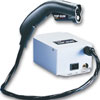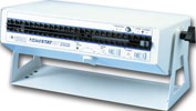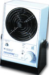
Ionisers play a crucial role in eliminating ESD damage in manufacturing and assembly operations surrounding electronic printed circuit board (PCB) systems.
While it is often assumed that the most common failure mode is as a result of the human body model (HBM) mechanism – where human beings become charged and subsequently discharge into ESD sensitive (ESDS) items – ESD damage is in fact most frequently caused by the charged device model (CDM) mechanism.
In the CDM failure mode, the ESDS device somehow becomes charged itself. For CDM damage to occur, the item becomes charged either from friction or by field induction. With field induction, the device becomes charged inductively simply by being in close proximity to the field. This phenomenon is not widely understood, but device charging can occur quite easily and rapidly by its introduction into a static charge field. For this reason, it is important to keep static generating material far away from ESDS items. If the ESDS item must be located near static generating material, ionisers are crucial to remove the hazards from the resulting field induction possibilities.
Applications
Conveyer transportation. All types of ESDS products (wafers, chips, substrates, components and PCB systems) can become highly charged via friction on improperly designed conveyor transport systems. It is important to verify that product charging does not occur in these conveyor systems or CDM damage is possible whenever the product contacts a conductor. Ionisers located over the conveyor at the inputs and outputs to handling machines have proved useful in these applications.
Bare PCBs. It is important to make sure that no charge exists on bare PCB assemblies, if active ESDS devices are about to be inserted onto them.
Automated PCB equipment. Wave solder, IC insertion, reflow solder, marking/inking and other PCB handling equipment can cause boards to charge up. Again, ionisers should be placed just before the PCBs receive contact with a conductor.
PCBs on platforms. Many operations place ESDS boards or systems on top of a platform of some kind – either at the workstation or on a conveyor. These platforms can and usually do insulate the ESDS item from ground and charging mechanisms are created that can only be eliminated via ionisation.
General purpose. As devices have become more vulnerable to electrostatic charge, it is recommended to install overhead ionisers at each location where board assemblies are handled. There are commonly a number of workstation operations where high charge generating plastic parts (such as connectors, cables, plastic housings, plastic lids and covers, plastic tubes, plastic panels etc) become mounted and handled at very close proximity to ESDS assemblies and boards. When plastic materials cannot be replaced by non charge generating alternatives, an ioniser is necessary to safely remove charging mechanisms in realtime as operators conduct the assembly process.


The following materials present a risk to ESDS items and boards when handled in close proximity to such items:
* Masking tape.
* Fibre-optic cables.
* Ribbon cables.
* Flex cables.
* Ordinary plastic connectors.
* Plastic housings for PCB.
* Final product plastic cases.
Air blow-off operations. Another very common charge generating mechanism in PCB assembly operations is the movement of air across the PCB material. Although ESD experts frequently disagree on whether it is the airflow itself or just the dust particles in the air that cause the charging, airflows in general are notorious for resulting in charged up PCBs. Ionising guns/blowers are a must for air blow-off operations on PCBs.
Plastic carts. It is highly recommended to eliminate any plastic carts from an electronic manufacturing facility. If they are still in use, however, ionisers should be employed if PCBs are being worked on in their presence.
Incoming inspection. In most facilities, there are occasions where ESDS items are received incorrectly packaged from a vendor and need to be repackaged in-house. In these cases, the ESDS item often becomes charged. It is good policy to have ionisers available at these incoming inspection sections so that incorrectly packaged ESDS items can be safely repackaged in ionised air.
PCB assemblies mounted onto plastic panels and into product cases. Perhaps the highest total value of documented damage to ESDS items has been caused by this failure mode. Specifically, many facilities mount their PCB assemblies onto high charge generating plastic panels in their final equipment designs. Under low humidity conditions these plastic panels become routinely charged to high levels (20–30 kV) when handled by operators. The PCB assembly circuits become charged inductively. The operators are then constantly discharging the assemblies via normal handling.
Test fixtures/sockets/prom burning sockets/burn-in boards. Test sockets and burn-in board fixtures are commonplace throughout test operations on devices at the component and board level. There are two separate possible CDM failure modes that have been verified to cause device damage. First, many of these sockets and high temperature sockets charge dramatically when handled by operating personnel, especially when they are wearing hand coverings. When the sockets have become charged, their relatively large surface area can produce fields that can cause inductive charging of the parts about to be inserted into them. The charged part can then be discharged upon contact with the socket pins. Damage to parts will be occurring just by placing parts into test sockets.
The second potential failure mode occurs if the sockets become highly charged; the resulting field can cause charging of the PCB wiring on the test or burn-in board. A discharge can then take place from the board to the device as it enters the socket. This second potential damage mode is actually a machine model (MM) failure mode. Bathing the sockets continually in ionised air during loading and unloading of the devices eliminates both failure modes.
Tape and reel construction operations. CDM failures have been determined in tape and reel operations. In almost all cases, damage can be traced to the presence of high charge generating rollers in the process near devices in the tape. Metal rollers are not typically charge generating sources but rollers covered with a plastic or rubber coating are tremendous charge generating sources. All charging from any rollers in this application should be eliminated either by charging the roller material or via ionisation.
Actum Electronics, in partnership with Simco, has field testers and ionisation equipment to ascertain exact charge readings in high risk areas, as well as the ability to supply the correct ionisation solutions.
| Tel: | +27 11 608 3001 |
| Email: | [email protected] |
| www: | www.actum.co.za |
| Articles: | More information and articles about Actum |

© Technews Publishing (Pty) Ltd | All Rights Reserved