


By their nature, FPGAs are power hungry devices with complex power delivery requirements and multiple voltage rails. A single chip commonly consumes multiple watts of power while operating from 1,8 V, 2,5 V and 3,3 V rails.
Activating high-speed on-chip SERDES can increase power consumption by several watts and complicate the power delivery strategy. When FPGA power consumption increases, performance requirements on sensitive analog and mixed-signal subsystems also increase. Chief among these are the clocking subsystems that provide low jitter timing references for the FPGA and other board-level components.
Power supply noise
Power hungry systems cannot be free of power supply noise. In general, system designers try to use low-noise linear power supplies whenever possible. However, excessive power dissipation usually prevents the use of linear regulators. When using a linear device, regulating from 3,3 V input to 1,8 V output is only 54% efficient, regardless of the load current. Low conversion efficiency burns power in the regulator instead of the load and makes linear devices unsuitable for many high-performance applications.
Low dropout regulators (LDOs)
The use of low dropout regulators (LDOs) helps improve efficiency by reducing the input-to-output voltage difference that the regulator produces. For example, 2,5 to 1,8 V regulation yields 72% efficiency for all loads. This is generally a good practice for loads up to 500 mA. However, when the load consumes 1 to 3 A of current, LDOs are less helpful. When a regulator enters dropout, it no longer regulates effectively. Its pass element behaves like a resistor, unable to respond to changes in load current or input voltage. This effect diminishes the noise rejection of the regulator, defeating the purpose of using it to provide power to sensitive circuit blocks.
To maintain good regulation and noise rejection, LDOs must be powered by considerably higher input voltages than their dropout specification dictates, decreasing efficiency. To avoid dropout conditions, multiple LDOs can be placed in parallel to reduce the load current through each regulator. Complicated and costly, this alternative is not an attractive solution.
Switching regulators
A more practical way to increase efficiency and maintain regulation over a wide load current range is with the use of switching regulators. The high 85% to 95% efficiency of switching regulators often makes them the only power conversion alternative for FPGAs. The boost in efficiency comes with a noise penalty, with as much as 50 to 100 mV of peak-to-peak voltage ripple. Due to the high power consumption of FPGA logic and I/O, switching ripple lower than 50 mVp-p is generally expensive and impractical.
Another noise source is the FPGA itself. The fabric system clock may run at tens to hundreds of megahertz. When high-power digital logic operates, it generates noise transients that ripple through the various power planes.
Fast transients create high energy spurs that power supply filters struggle to smooth out. Since most power supply decoupling is optimised to present low impedance around one or a few frequencies, it is difficult or even impossible to clean up all high-frequency noise on the power supply rail. This noise tends to propagate to other subsystems through the power supply, especially those in close proximity with the FPGA.
Load droops
FPGAs present another challenge. When blocks of logic or I/O switch between low- and high-power operating states, the load current fluctuates dramatically. As the logic blocks enter a high-power operating state where the logic undergoes intensive processing, the power supply tends to experience a load droop. As the logic block transitions to a lower power state, the load droop disappears and the power rail returns to a nominal state.
Multiple events can create such a load droop and the overall interaction of these events is generally impossible to predict or control. Such load variation creates a lowfrequency envelope on the rail that is generally much less than 100 kHz. This noise envelope can be cleaned up using additional regulators, but this adds cost and board space and may reduce power supply operating margin.
Sharing power rails
For these reasons, sensitive analog components tend to present a challenge when sharing the same power rails as FPGAs. In many cases, users may experience unexplained performance degradation or anomalous, unpredictable behaviour. The traditional solution is to isolate each sensitive timing subsystem on its own power island using linear regulators to filter low-frequency noise and extensive LC filtering using ferrite beads and ceramic decoupling capacitors to cover higher frequencies.
However, this is not an ideal solution because it adds cost and increases layout complexity. Furthermore, it breaks up the power planes, reducing their effectiveness in providing low impedance and tightly coupled ground return. A better solution is to maintain a continuous power plane that remains as intact as possible throughout the board. However, in order to take advantage of this, each subsystem must be able to tolerate noise on the power supply.
Using crystal oscillators
Today’s FPGAs depend heavily on low-jitter clock sources to meet end application requirements. FPGAs may drive backplanes, optical modules or GMII/XGMII interfaces, all of which require extremely low-jitter timing references. Operating in the noisy environment that FPGAs create has become a major challenge for FPGA reference clocks.
Figure 1a and Figure 1b show two types of crystal oscillators. Crystals have been used for decades to set the heartbeat of most electronic systems. They provide low phase noise, good frequency accuracy and adequate performance for many high performance applications. Despite these advantages, crystals have a major limitation: fundamental frequency oscillation is limited to frequencies lower than 50 MHz. For most high performance applications, the crystal must be followed by a PLL that multiplies the low-frequency reference by the appropriate amount to generate the output frequency of interest. PLLs are used to multiply the initial frequency by an integer value such as 3 or a fractional value such as 3,125.
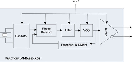
The fractional-N topology of Figure 1a is comprised of a crystal oscillator followed by an analog phase detector, analog compensation filter, analog VCO and a fractional-N feedback divider. The output frequency equals the input frequency scaled by the ratio 1/N. A low-noise buffer is used to drive the external load circuitry. Many applications such as Gigabit Ethernet, Fibre Channel and high definition serial digital video (HD-SDI) rely on low-jitter clock sources with output frequencies ranging from 100 to 156,25 MHz.
Under ideal supply conditions, a fractional-N PLL can be designed to provide good jitter performance of less than 1 ps RMS integrated over the 10 kHz to 20 MHz band. In contrast, in an environment with a noisy power supply, an oscillator may struggle to meet the phase jitter specified in the datasheet. Using analog sub-circuits creates vulnerable nodes where noise can be injected. When noise enters the system, it often becomes amplified, generating output phase jitter.
Using DSPLL-based oscillators
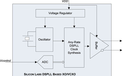
In contrast, the Silicon Labs DSPLL-based approach uses digital processing to implement a PLL that multiplies the crystal reference frequency to a higher frequency. The crystal is never pulled. All frequency control and trimming is carried out using digital commands. The compensation filter is based on a digital signal processor that does not use capacitors or other passive components. Finally, the VCO is controlled digitally without using analog circuitry.
To offer additional VDD isolation, an on-chip linear regulator and in-package power supply decoupling capacitor are used to further ensure noise rejection. Due to these advancements, every Silicon Labs DSPLL-based XO/VCXO has the ability to generate high-frequency clock signals with sub-picosecond jitter performance in noisy real-world environments.
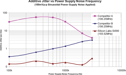
Figure 2 shows the power supply rejection ratio performance of fractional-N PLL-based XOs compared to Silicon Labs DSPLL-based XOs. Although fractional-N PLL-based XO is rated to achieve 0,9 ps maximum RMS jitter, suitable for high data rate FPGA SERDES, the rated specification applies only in ideal environments. With 100 mVp-p of power supply noise, competing solutions generate up to 40 ps RMS of additive jitter, becoming unusable in high-speed serial links. Silicon Labs DSPLL-based XO/VCXO products do not suffer from this limitation, adding only 0,1 to 0,3 ps RMS of jitter across the tested frequencies.
Other DSPLL timing devices offered by Silicon Labs are low-jitter, integrated PLLs used for jitter attenuation and clock multiplication. These devices also employ a DSPLL-based architecture that eliminates VDD noise sensitivity.
When using the Si5xx XO/VCXOs or Si53xx family of any-rate clock multipliers, designers can take advantage of high-efficiency switching power supplies while maintaining excellent jitter performance. In addition, designers are free to implement continuous power and ground planes without the need to sprinkle linear regulators around the board, offering a low-impedance, minimally interrupted ground plane design. On-chip power regulation enhances system performance, minimises board area, reduces system cost, simplifies design and improves time-to-market.
Conclusion
In conclusion, today’s FPGA–based designs require improved clocking with greater immunity to power supply switching noise observed in real-world applications. With low jitter that meets high-speed serial link requirements and integrated power supply noise rejection that optimises operation under real-world conditions, Silicon Labs’ family of DSPLL-based clocks and oscillators is a desitable complement to FPGAs in high-performance applications.
For more information contact Gary de Klerk, NuVision Electronics, +27 (0)11 894 8214, [email protected], www.nuvisionelec.co.za
| Tel: | +27 11 608 0144 |
| Email: | [email protected] |
| www: | www.nuvisionelec.com |
| Articles: | More information and articles about NuVision Electronics |


© Technews Publishing (Pty) Ltd | All Rights Reserved
 printer friendly version