


Jitter analysis has been a hot topic in the test and measurement world for several years now.
Measurement tools have steadily improved, allowing engineers to easily assess just how big their jitter problems are, as well as what types of jitter they are confronted with. Because the main reason that engineers care about jitter is that it causes bit errors, it is important to view jitter from a system level perspective. Only knowing how big the problem is does not necessarily provide an engineer with the information needed to improve system level or even component level performance.
Solving jitter problems requires a multipronged approach. First, it is important to measure the jitter performance at the transmitter to gauge just how big the problems are. If problems exist, it is important to then examine the reference clocks that drive the transmitters, as they are the fundamental source of system timing. Frequency domain clock analysis can provide the telltale ‘root cause’ clues that can be obscured in traditional time-domain jitter analysis. It then becomes important to see how the clock jitter actually manifests itself onto the data signals. Finally, jitter can never be completely removed. It is then necessary to take what has been learned about the clock and transmitter to design a receiver that can tolerate the expected signal jitter.
This article reviews the process of analysing the components of a digital communications system with an emphasis on understanding how the different components interact. Techniques for identification of root causes for jitter are investigated.
How jitter manifests itself in a communications system
Jitter can come from a variety of sources. It is useful to examine the basic architecture of a generic serial data system and discuss the mechanisms that create jitter within each element. Just as important is understanding how jitter from one element can affect the jitter performance of another element.
The basic digital communications system consists of a transmitter, a channel, a receiver, and often some form of a reference clock. The system described is intended to be generic and represent distributed, forward and embedded clock architectures.
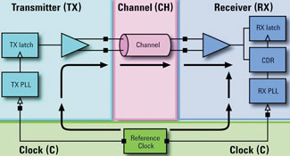
Reference clocks
The reference clock determines the data rate of the serial bus system. If the reference clock fluctuates in frequency, the data rate of the system will also fluctuate or jitter. Jitter mechanisms in the reference clock include random jitter from noise mechanisms within the oscillator, periodic jitter from spurious oscillator sidebands, and duty cycle distortion from oscillator nonlinearities.
Transmitters
To produce data, the transmitter derives its timing from a clock source. The transmitter typically multiplies up the reference clock to achieve the desired data rate. The multiplication is usually achieved with some form of phase-locked loop (PLL). In the process of multiplication, the PLL will add some jitter – typically random jitter from its internal oscillator. The jitter from the reference clock may also be imposed on the multiplied clock. The transmitter can also have jitter from mechanisms that are not related to the reference clock, including random jitter from thermal effects, inter-symbol interference from limited bandwidth, and periodic jitter due to electromagnetic interference.
Channels
The channel can alter the time at which a signal crosses the ideal decision threshold (another way to describe jitter). This is typically due to limited bandwidth and is commonly referred to as inter-symbol interference.
Receivers
Receivers can also produce jitter as there may be PLLs or other timing elements that are subject to random jitter mechanisms. Typically jitter analysis for a receiver deals with the ability of the receiver to achieve a good bit-error-ratio in the presence of jitter, rather than determining the amount of jitter that is created. However, if a receiver obtains its timing information from a reference clock, the receiver can be subject to similar jitter transfer and amplification issues as the transmitter.
When jitter becomes large enough, it can cause receivers to make mistakes and degrade the BER of a communications system. To minimise the effects of jitter, it can be reduced at the point it is created, or it can be managed at downstream points in the signal path. In either approach, the more that is known about the jitter, the better the chances that it can be dealt with efficiently.
Using frequency domain jitter analysis to solve jitter problems: a case study
Reduction of jitter requires identification of its root causes. High-speed digital engineers have learned the benefits of separating jitter into its random and deterministic components, both for accurate assessment of total jitter to low probabilities as well as identification of jitter sources. While jitter separation techniques can be used to determine the types of jitter that exist on clock or data signals, additional information is often needed to determine where jitter originates and provide insight into how system performance can be improved.
Figure 2 shows the jitter measurement results for a PCI-Express data signal. The total jitter (TJ) at a probability of 10-12 is 175 ps or 0,44 unit intervals (UI). There are several significant contributors to the jitter. Data dependent (DDJ) effects including ISI (inter-symbol interference) and duty-cycle distortion (DCD) are relatively small. Periodic jitter (PJ) is significant, and the random jitter (RJ) is large. (Because the RJ is listed as a root-mean-square value assumed to represent the standard deviation of a Gaussian distribution, its impact on the TJ at a 10-12 probability level requires it be multiplied by ~ 14 standard deviations, making it the largest contributor).
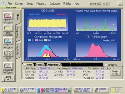
Where does the jitter come from? This is the critical question that must be answered if the jitter is to be reduced. The DCD can be due to DC offsets or differences in rise and fall times of signal edges. ISI can be due to device or channel bandwidth limitations. Both DCD and ISI effects are relatively easy to observe on the time domain waveform and can often be diagnosed with an oscilloscope. The largest jitter mechanisms in this example, PJ and RJ, can also be observed with an oscilloscope, but it can be difficult to see the details necessary to get root causes.
Using frequency domain techniques to observe the jitter spectrum provides a wealth of information on periodic and random jitter that can be difficult, if not impossible, to obtain in the common time domain view. What does jitter look like in the frequency domain?
The ideal reference clock oscillator will produce a simple sinusoid at the desired frequency:
Videal(t) = vosin 2πfct
In the time domain, this signal is seen as the basic sine function. In the frequency domain, the signal is seen as a single spectral line at the frequency of the sinusoid.
No oscillator is perfect. A real oscillator will produce a signal described by:
Vreal(t) = (vo + Δv(t))sin (2πfct + φ(t))
Where:
Δv(t) represents signal fluctuation due to amplitude noise
φ(t) represents fluctuations in the phase of the clock signal.
In the time domain, this signal will fluctuate in amplitude and have an inconsistent period. In the frequency domain, the signal is no longer a discrete spectral line. There is now spreading of the spectrum – unintentional amplitude and phase modulation causing spectra both above and below the nominal signal frequency. If the modulation is due to a random source, the spectrum spreads across a continuous range of frequencies. If the modulation is periodic, there will be discrete modulation sidebands offset from the original centre frequency.
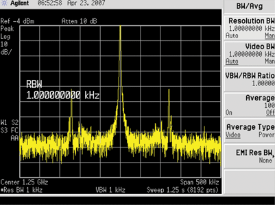
To understand how a signal has been degraded by jitter, it is helpful to examine the frequency domain spreading of the signal in detail. The spread of the clock spectrum is typically symmetric ie, the spectrum above the main signal is a mirror image of the spectrum below the main signal. A useful approach is to simply look at the upper modulation alone, in terms of its offset position from the ideal signal (carrier). If the spread is dominated by random noise processes, a handy approach to assess the magnitude of the problem is to quantify the sideband energy over a specific spectral width, typically 1 Hz. This is commonly referred to as a phase noise plot, which is a display of the phase modulation of a signal, plotted as the energy of the signal in a 1 Hz bandwidth compared to the total energy of the signal.
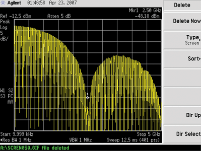
Another way to observe jitter in the frequency domain is the jitter spectrum plot. In contrast to a phase noise plot, the jitter spectrum plots the magnitude in seconds (rms) and the data is not normalised for the measurement resolution. Digital link designers generally prefer this representation since the jitter is absolute, allowing direct comparison of two signals at different rates such as a sub rate clock compared to a full rate clock. The jitter spectrum can preserve phase information so that any deterministic components of the spectrum (such as spread-spectrum clocking or SSC) can be processed and reconstructed in the time domain. The random noise can also be integrated to get the total rms random jitter. This allows construction of a probability density functions required for BER estimations.
| Tel: | +27 12 678 9200 |
| Email: | [email protected] |
| www: | www.concilium.co.za |
| Articles: | More information and articles about Concilium Technologies |


© Technews Publishing (Pty) Ltd | All Rights Reserved
 printer friendly version