


The PCB design guidelines presented in this article are formulated to offer the following benefits:
* Effective power supply decoupling is provided by placing ceramic capacitors next to the IC with minimum length connection traces.
* Short PCB traces and ground planes reduce RF susceptibility and radiated emissions.
* Robust ESD and EMI protection is achieved by placing transient voltage suppressor (TVS) diodes next to the I/O connector.
Decoupling capacitors
Decoupling capacitors increase the noise immunity level of a translator by reducing the supply voltage droop. The capacitors filter and bypass noise signals on the power supply voltage lines to ground. These transients are due to the high peak but short duration switching transients that can cause problems such as glitches on the output voltage signals.
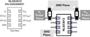
Figure 1 provides an example of the recommended locations of the VL and VCC decoupling capacitors. Ceramic capacitors with a magnitude of 0,01 μF to 0,1 μF are a good choice because they are inexpensive, small and have excellent high-frequency attenuation specifications. Ground and power planes are one option commonly used to provide short, low impedance trace connections.
Minimising the loop area
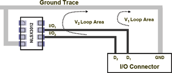
Figure 2 shows that the translator’s I/O1 and I/O2 traces form a loop with the ground trace. The loop area functions as an antenna that allows high-frequency noise to enter (susceptibility) and leave (emissions) the PCB. Furthermore, RF susceptibility and emissions are proportional to the size of the loop and the frequency or bandwidth of the signals.
The bandwidth of a digital signal is produced by the fast rise and fall times and can be approximated as
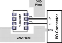
RF susceptibility and radiated emissions can be reduced by minimising the loop area formed by high-speed data and ground lines. The first step is to shorten the translator’s I/O-to-connector trace lengths. Next, incorporating a ground plane in the PCB design will reduce the loop area. Loop problems can also be minimised by slowing the edge rate of the signals; however, this approach typically is not an option because translators have a relatively modest output current specification. Figure 3 shows a layout that can be used to reduce the translator’s RF susceptibility and emissions.
TVS diode protection devices
Why are TVS devices required?
TVS devices typically are not required for internal PCB translations; however, they should be used for external module-to-module applications. Translators that are connected to I/O connectors are exposed to potentially harmful ESD and EMI surge voltages. The power supply and data cables plugged into the I/O connector are common entry points for conducted and coupled transient surge voltages. Also, the parasitic cable capacitances and inductances provide a path for power line surge voltages to be coupled into the data lines.
Voltage translators typically have a much higher ESD rating then a conventional logic IC; however, their immunity level for other surge pulses is not specified. In contrast, TVS diodes have a higher ESD rating and are specified for longer duration, higher energy surge pulses. The surge ability of a TVS device is proportional to die size and it is not practical to incorporate large protection devices inside an IC. The translator’s small protection devices can reliably withstand only a limited number of low energy, short duration surge events such as ESD. In contrast, external TVS devices have a relatively large die size and are designed to withstand very high ESD levels and repetitive, long duration transient surge voltages.
TVS PCB layout guidelines
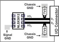
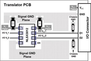
Only a few design layout rules are needed for TVS diodes to increase the translator’s ability to suppress surge voltages. Figure 4 provides a graphical representation of the layout recommendations.
The PCB design guidelines include:
* Locate the TVS devices close to the I/O connector.
* Connect the surge protection circuits to chassis or power ground.
* Select surface mount TVS devices.
Location
TVS devices should be located close to the connector with short, low-impedance connection traces. If the TVS diode and internal IC protection circuits have a similar turn-on voltage, the impedance of their PCB traces will be the key factor that determines where the surge energy will be dissipated. The close proximity of the TVS devices to the connector results in a trace impedance that is less than the translator-to-I/O connector trace. This ensures that the surge current will be dissipated by the external TVS devices rather than by the translator’s internal protection circuit.
Ground options
The TVS devices should shunt the surge voltage to chassis ground rather than signal ground. Shunting the surge voltage directly to the translator’s signal ground can cause ground bounce. PCBs that have a single ground can minimise the TVS device’s ground connection impedance by using ’stub’ traces that are relatively short and wide.
Package selection
A small TVS device usually has better EMI characteristics than a device housed in a larger leaded package. The inductance of a TVS diode is proportional to its size; thus, a small SMT package reduces the magnitude of the voltage spike that is produced by the V = L ΔI/Δt inductance term. In addition, inductance degrades the high-frequency attenuation characteristics of the TVS device.
TVS diode selection guidelines
Diode arrays and avalanche TVS diodes provide a simple, low cost solution to protect the translator’s I/O pins. A TVS device can also be used on the power line associated with the I/O connector; however, the decoupling capacitor typically is adequate. Additional details on TVS diodes are provided in references [1] and [2].
Diode array protection circuit
Figure 5 provides an example of a diode array protection circuit. Diodes arrays steer the surge current into the ground and power supply planes to dissipate the energy of the transient voltage pulse. The main advantage of the array is that the capacitance of a switching diode is low and will not distort a high-speed digital signal. Diode arrays such as the NUP1301, with a capacitance of less than 1 pF, are readily available.
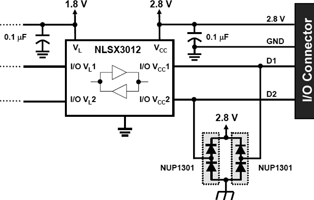
The main disadvantage of the diode array circuit is that a potential for back drive can exist. Back drive occurs when a path exists for current to flow through the diode array via a data line. The data line connecting the two modules can unintentionally provide power to ICs that are connected to the power rail if the voltage at the I/O connector is greater than VCC. This condition can cause power-up problems and anomalies such as the illumination of indicator lights on an unpowered PCB.
Avalanche TVS diode protection circuits
Avalanche TVS diodes do not have a back drive problem because they clamp the surge voltage to ground and do not have a path to VCC. Figure 6 provides an example of a unidirectional avalanche circuit, while Figure 7 shows a bidirectional circuit. In most applications, either uni- or bi-directional TVS devices can be used to protect the translator. In general, a bidirectional avalanche diode will have a lower capacitance than a unidirectional device, but a larger capacitance than a diode array.
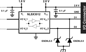

Designers often incorrectly believe that the negative symmetrical clamping voltage of a bidirectional TVS device violates the ‘maximum rating’ table of a translator. Most translators have a specified minimum value equal to -0,5 V. The datasheet rating is not violated because the voltage at the power and I/O pins is specified for DC steady-state value and is not applicable for a transient pulse with a duration that is usually less than 1 μs.
Summary
Figure 8 provides a graphical representation of the recommended PCB layout guidelines for a dual supply voltage translator. A multilayer PCB provides a simple method to incorporate power and ground planes into the layout design. Typically, signal traces are located on the top and bottom layers, while the power and ground planes are located on separate internal layers.
The key PCB design guidelines include:
* Locate the decoupling capacitors as close as possible to the power pins.
* Provide ground and power planes to minimise the PCB trace lengths.
* Use short I/O traces and ground planes to decrease RF susceptibility and radiated emissions.
* Locate avalanche TVS diodes next to the I/O connector to enhance the translator’s ESD and EMI immunity.
Bibliography
1. Lepkowski, J., ‘AND8231 - Circuit Configuration Options for TVS Diodes’, ON Semiconductor, 2005.
2. - , AND8232 - PCB Design Guidelines that Maximise the Performance of TVS Diodes, ON Semiconductor, 2005.
| Tel: | +27 11 923 9600 |
| Email: | [email protected] |
| www: | www.altronarrow.com |
| Articles: | More information and articles about Altron Arrow |


© Technews Publishing (Pty) Ltd | All Rights Reserved
 printer friendly version